 Menu
Menu


PCB Fab House
-
Min Order
1
-
Product Unit
Pieces
-
Origin
China Mainland
-
Payment


- Contact Now Start Order
- Favorites Share
- Description
Product Detail
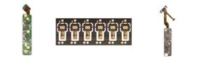
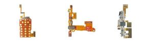
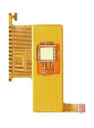
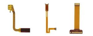
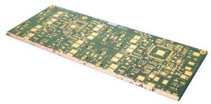
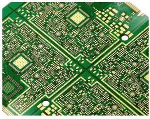
Multi layer
Product design, system speed requirements, microprocessor and component scaling, and increased thermal performance are driving advances in PCB technology every day. Hemeixin’s technical and production capability and aggressive technology roadmap has kept pace with these changes and provides a scalable platform for growth.
• Layers (2-64)
• Lines and Spaces (Volume 3/3 Prototype 2/2)
• Controlled Impedance (+/- 10% Standard - +/- 5% Advanced)
• Blind and Buried Vias; Filled via capability
• Buried Capacitance
Dielectric thickness: 14 µm
Capacitance /area: 6.4 nF/in2
Breakdown Voltage: >100V
3M material, no need license
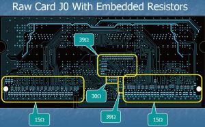
• Buried Resistor
Resistance (ohms/sq.) : 25, 50, 100, 200
• Advanced thermal management and embedded coin technology
• High Performance and Emerging Materials; Halogen free,low loss,ultra-thin,mixed packages, inlay
• Sequential Lamination
• High Tech Drilling Capability – Small hole drilling, Backdrilling
• Mechanical depth control drilling with +/-10um tolerance,min drill
size 0.15mm
• Ultra Fine Pitch (0.8, 0.5, 0.4, 0.3 mm)

Solution


-
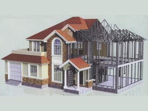
Prefab Steel Hangar 1 Pieces / (Min. Order)
-
Steel Prefab House 1 Pieces / (Min. Order)
-
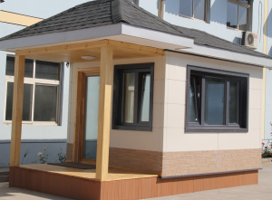
Cement Prefab House 1 Pieces / (Min. Order)

-
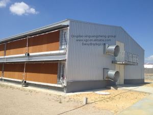
Prefab Poultry House 1 Pieces / (Min. Order)
-
Poultry Farm House 1 Pieces / (Min. Order)
-
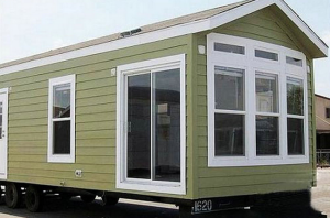
Prefab Container House 1 Pieces / (Min. Order)
-
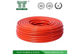
PVC Gas Hose 1 Pieces / (Min. Order)
-
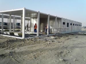
Prefab House Labor Camp 1 Pieces / (Min. Order)

-
Prefab houses for sale in kenya 1 Pieces / (Min. Order)
-
Prefabricated houses south africa 1 Pieces / (Min. Order)

-
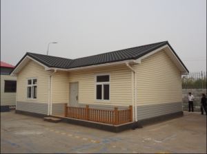
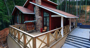
Prefab homes 1 Pieces / (Min. Order)

-
Prefabricated house in saudi arabia 1 Pieces / (Min. Order)
-
Prefabricated House-P-1-001 1 Pieces / (Min. Order)
-
Prefabricated House-P-1-002 1 Pieces / (Min. Order)
-
Prefabricated House-P-1-003 1 Pieces / (Min. Order)
 Favorites
-
 Sunstone PCB
1 Pieces / (Min. Order)
Sunstone PCB
1 Pieces / (Min. Order)
-
 PCB Creation
1 Pieces / (Min. Order)
PCB Creation
1 Pieces / (Min. Order)
-
 PCB Cost B
1 Pieces / (Min. Order)
PCB Cost B
1 Pieces / (Min. Order)
-
 PCB Makers
1 Pieces / (Min. Order)
PCB Makers
1 Pieces / (Min. Order)
-
 PCB Cost A
1 Pieces / (Min. Order)
PCB Cost A
1 Pieces / (Min. Order)
-
 PCB Suppliers
1 Pieces / (Min. Order)
PCB Suppliers
1 Pieces / (Min. Order)
 Frequent updates ensuring high quality data
 Over 5000 customers trust us to help grow their business!


 Menu
Menu