 Menu
Menu


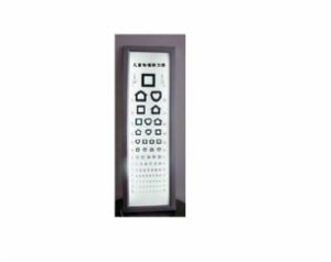
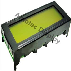
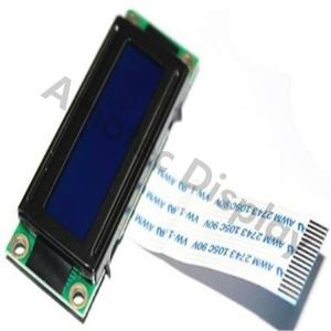
High Contrast LCD Display
-
Min Order
1
-
Product Unit
Pieces
-
Origin
China Mainland
-
Payment


- Contact Now Start Order
- Favorites Share
- Description
Product Detail
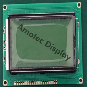
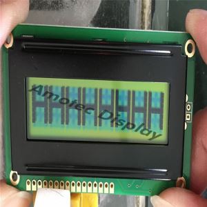
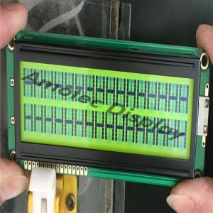
High contrast lcd display
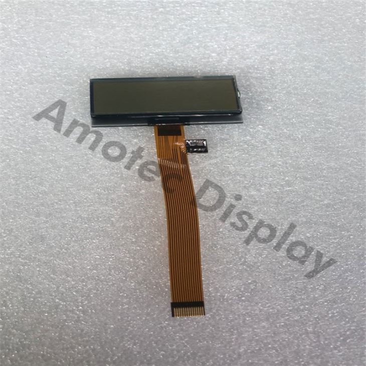
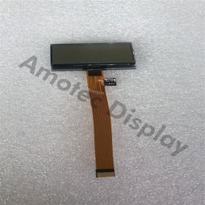
High contrast lcd display ADG16064A0
Model No.ADG16064A0
? High contrast lcd display 160x64, Display LCD160x64
? Monochrome Graphic LCD
? Built-in controller ST7525i-G4.
? 1/65 Duty, 1/9 Bias
Description of High contrast lcd display ADG16064A0
High contrast lcd display ADG16064A0 is a dot matrix graphic LCD module which is fabricated by low power COMS technology. It can display160Dots × 64 dots graphic LCD panel. The High contrast lcd display ADG16064A0 combines FSTN /GRAY, Positive, Transflective with RGB backlight.
1. FEATURES
The features of LCD are as follows
* Display mode : FSTN /GRAY, Positive, Transflective
* Color : Display dot :Blue-Black
Background: GRAY
* Display Format : 160Dots × 64Dots graphic
* IC : ST7525i-G4.
* Interface Input Data :I2C
* Driving Method : 1/65 Duty, 1/9 Bias
* Viewing Direction : 6 O’clock
* Backlight : LED(Red-Green-Blue)
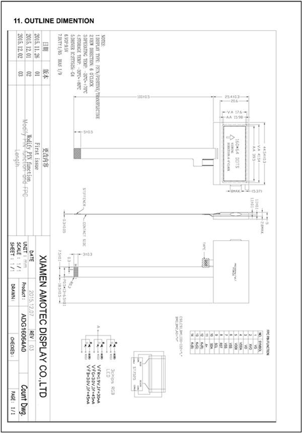
2. MECHANICAL SPECIFICATIONS
| Item | Specification | Unit |
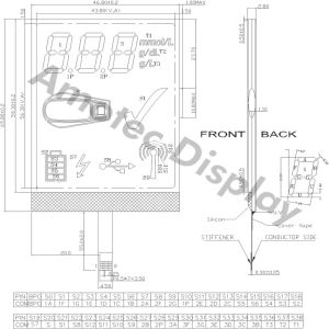
Module Size | 44.54(W) X25.4(H) X5(T) | mm |
Viewing Area | 41.54(W) X 17.6(H) | mm |
Effective Display Area | 39.5(W) X15.98(H) | mm |
Number of Dots | 160 X 64 Dots | - |
Dot Size | 0.227(W) X 0.223(H) | mm |
Dot Pitch | 0.247(W) X 0.25(H) | mm |
3. ELECTRICAL SPECIFICATIONS
3-1. Absolute Maximum Ratings (Vss=0V)
| Item | Symbol | Standard Value | Unit | ||
Min. | Typ. | Max. | |||
Supply Voltage For Logic | VDD | -0.3 | - | 4.0 | V |
Supply Voltage For LCD Drive | V0-XV0 | -0.3 | - | +13.5 | V |
Operating Temp. | TOP | -20 | - | +70 | °C |
Storage Temp. | TST | -30 | - | +80 | °C |
Static Electricity | Be sue that you are ground when handing LCM | ||||
3. ELECTRICAL SPECIFICATIONS
3-2-1.Electrical Characteristics
Item | Symbol | Test | Min. | Typ. | Max. | Unit | |
Supply Voltage For Logic | VDD – VSS | Ta=25? | 2.7 | 3.1 | 3.3 | V | |
Supply Voltage For LCD | V0 – XV0 | Ta=25? | 9.3 | 9.5 | 9.7 | V | |
Input Voltage | “H” Level | V IH | Ta=25? | 0.8VDD | - | VDD | V |
“L” Level | V IL | VSS | - | 0.2VDD | V | ||
Output Voltage | “H” Level | V OH | IOUT= -0.5mA | 0.8VDD | - | VDD | V |
“L” Level | V OL | IOUT= 0.5mA | VSS | - | 0.2VDD | V | |
Current Consumption | IDD | VIN = VDD | - | 1.6 | 2.0 | mA | |
NOTE: 1) Duty ratio=1/65, Bias=1/9
2) Measured in Dots ON-state
3-3. BACKLIGHT
3-3-1. Absolute Maximum Ratings
Item | Symbol | Condition | Min. | Typ. | Max | Unit |
Forward Current | IF | Ta= 25? | - | - | 30 | mA |
Reverse Voltage | VR | - | - | 5 | V | |
Power Dissipation | PD | Ta= 25? | - | - | - | mW |
3-3-2. Opto-electronic Characteristics
Item | Symbol | Condition | Min. | Typ. | Max | Unit |
Forward Voltage(Ta= 25?) | VF(RED) | IF=30mA | 1.9 | - | 2.2 | V |
VF(GREEN) | IF=45mA | 2.8 | - | 3.2 | ||
VF(BLUE) | IF=45mA | 2.8 | - | 3.2 | ||
Luminous | - | - | - | - | - | cd/m² |
4. Interface Pin Function
Pin NO. | Symbol | I / O | Functions |
1 | VG | p | LCD driving voltage for segments. |
2 | XVO | p | LCD driving voltage for commons at positive frame. |
3 | VO | p | LCD driving voltage for commons at negative frame. |
4 | VDDA | p | Digital power. If VDD1=VDD2, connect to VDD2 by ITO. |
5 | VDDI | p | Analog power. If VDD1=VDD2, connect to VDD1 by ITO. |
6 | VSS | p | POWER GROUND |
7 | VSS | p | POWER GROUND |
8 | RST | I | Reset input pin. |
9 | SCL | I/O | When using I2C interface |
10 | SDA | I/O | |
11 | A+ | p | POWER FOR BACKLIHT(ANODE) |
12 | K-(R) | p | POWER FOR BACKLIHT(CATHODE) Red |
13 | K-(R) | p | POWER FOR BACKLIHT(CATHODE) greed |
14 | K-(R) | p | POWER FOR BACKLIHT(CATHODE) blue |
FAQ
1.What is RAM Interface
Answer :The external RAM is used to store display data( text, graphic and external CG data ). It can be freely allocated to the memory area( 8 K byte max ).
2.Can graphic LCD module display characters?
A graphic LCD display module is typically required when the display of more than just text is required. Many of the LCD controllers on board also include a CGROM (character generator ROM) to be able to easily use character as well as graphics.
3.What can graphic LCD display ?
This Graphic LCD display module is 160x64 graphic mode --or-- Character Generator mode (Character font) optional.
4.What are the precautions in use of LCD Modules?
(1)Avoid applying excessive shocks to the module or making any alterations or modifications to it.
(2)Don’t make extra holes on the printed circuit board, modify its shape or change the components of LCD module.
(3)Don’t disassemble the LCM.
(4)Don’t operate it above the absolute maximum rating.
(5)Don’t drop, bend or twist LCM.
(6)Soldering: only to the I/O terminals.
-
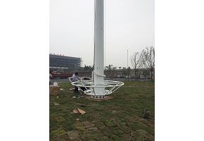
Single Mast Lift Platform 1 Pieces / (Min. Order)
-
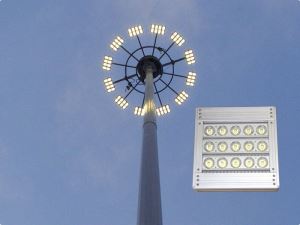
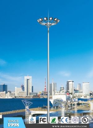
High Mask LED Light 1 Pieces / (Min. Order)
-
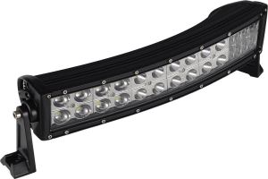
high intensity Epistar LEDS light bars 1 Pieces / (Min. Order)
-
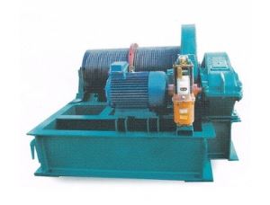
High Lift Winch Type 1 Pieces / (Min. Order)
-
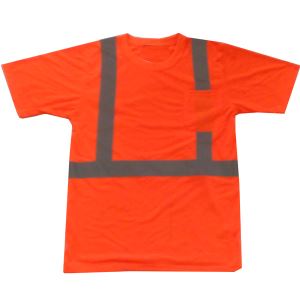
High Visibility Work Shirts 1 Pieces / (Min. Order)
-
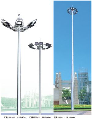
high mast lighting 1 Pieces / (Min. Order)
-
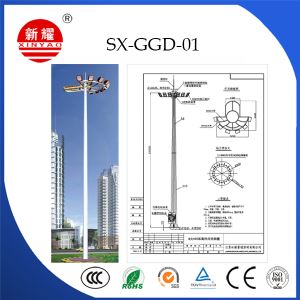
High Mast Lighting Pole 1 Pieces / (Min. Order)
-
High Mast Lighting Tower 1 Pieces / (Min. Order)
-
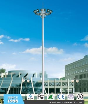
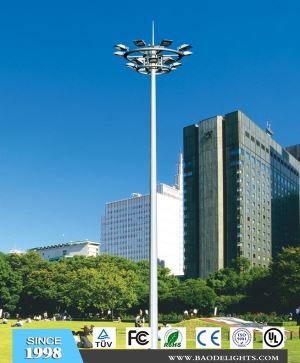
High Mast 1 Pieces / (Min. Order)
-
High Mast Pole 1 Pieces / (Min. Order)
-
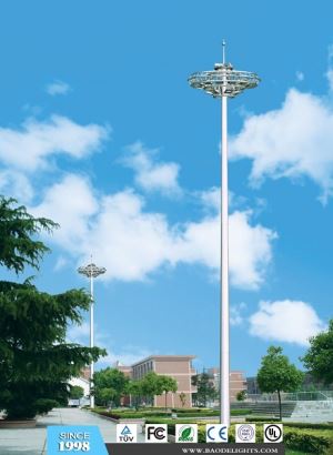
High Mast Lamp 1 Pieces / (Min. Order)
-
High Mast Light 1 Pieces / (Min. Order)
-
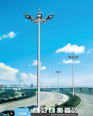
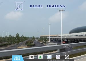
High Mast Stadium Light Tower Poles 1 Pieces / (Min. Order)
-
High Mast Lighting Poles 1 Pieces / (Min. Order)
-
Visual Chart Light Box 1 Pieces / (Min. Order)
-
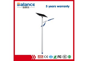
high lumen 12v solar led street light 1 Pieces / (Min. Order)
-
High Mast LED Light Pole 1 Pieces / (Min. Order)
-
High Post Light 1 Pieces / (Min. Order)
-
High Mast Light 1 Pieces / (Min. Order)
 Favorites
-
 TFT LCD 7 Monitor
1 Pieces / (Min. Order)
TFT LCD 7 Monitor
1 Pieces / (Min. Order)
-
 Graphic LCD Smart Display
1 Pieces / (Min. Order)
Graphic LCD Smart Display
1 Pieces / (Min. Order)
-
 Industrial LCD Panel
1 Pieces / (Min. Order)
Industrial LCD Panel
1 Pieces / (Min. Order)
-
 LCD Graphic Display 128x64
1 Pieces / (Min. Order)
LCD Graphic Display 128x64
1 Pieces / (Min. Order)
-
 Low Power LCD Display
1 Pieces / (Min. Order)
Low Power LCD Display
1 Pieces / (Min. Order)
-
 Character LCD Display Panel
1 Pieces / (Min. Order)
Character LCD Display Panel
1 Pieces / (Min. Order)
-
 Digital LCD Display
1 Pieces / (Min. Order)
Digital LCD Display
1 Pieces / (Min. Order)
 Frequent updates ensuring high quality data
 Over 5000 customers trust us to help grow their business!


 Menu
Menu