 Menu
Menu


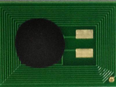
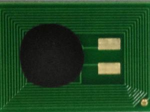
Trigger NFC
-
Min Order
1
-
Product Unit
Pieces
-
Origin
China Mainland
-
Payment


- Contact Now Start Order
- Favorites Share
- Description
Product Detail
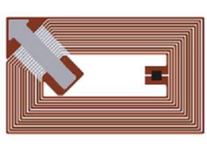
1. General Description
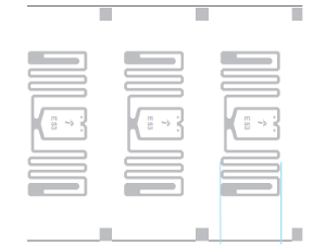
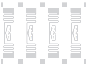
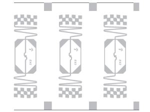
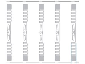
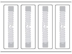
YFNFC02B is a small form factor NFC tag (RFID) module for consumer or PC peripheral devices. With the printed antenna on the module, the user can use it easily to be the short distant tag (up to 62.5px). With those 2 pins connecting to a trigger circuit, it can act as a pairing mechanism for Bluetooth Simple Secure Pairing device.
Contactless Interface
• Physical Interface and Anticollision compliant to ISO/IEC 14443-3 Type A
– Operation frequency 13.56 MHz
– Data rate 106 kbit/s in both direction
– Contactless transmission of data and supply energy
– Anticollision logic: several cards may be operated in the field simultaneously
• Unique IDentification number (7-byte double-size UID) according to ISO/IEC 14443-3 Type A
• Read and Write Distance up to 2.5 cm and more (influenced by external circuitry i.e. reader)
152 bytes EEPROM
• Organized in 38 blocks of 4 bytes each
• 128 bytes freely programmable User Memory
• 24 bytes of Service Area reserved for UID, Configuration, LOCK Bytes, OTP Block and Manufacturer Data
• Read and Write of 128 bytes of User Memory in less than 100 ms
• Programming time per block < 4 ms
• Endurance minimum 10,000 erase/write cycles)
• Data Retention minimum 5 years)
Privacy Features
• 32 bit of One Time Programmable (OTP) memory area
• Locking mechanism for each block
• Block Lock mechanism
• Optional 32 bit Password for Read/Write or Write access
• Optional Password Retry Counter
• Optional 16 bit Value Counter
Data Protection
• Data Integrity supported by 16 bit CRC, parity bit, command length check
• Anti-tearing mechanism for OTP, Password Retry Counter and Value Counter
Support
• ISO/IEC 14443-3 Type A
• ISO/IEC 18092
• NFC Forum™ Type 2 Tag Operation
2. Application
Bluetooth Secure Simple Pairing Using NFC
• Bluetooth mouse
• Bluetooth keyboard
• Bluetooth headset
• Bluetooth speaker
• Other Bluetooth device
3. Circuit Description
• Analog Contactless Interface
–The Analog Contactless Interface contains the voltage rectifier, voltage regulator and system clock to supply the
IC with appropriate power. Additionally the data stream is modulated and demodulated.
• Memory Unit
– The Memory Unit consists of 38 blocks of 4 bytes each.
• Control Unit
–The Control Unit decodes and executes all commands. Additionally the control unit is responsible for the correct anticollision flow.
4. Memory Principle
The total amount of addressable memory is 152 bytes organized in blocks of 4 bytes each.
The general structure comprises Service Areas as well as User Areas:
• 24 bytes of service and administration data (located in Service Area 1 and 2) reserved for
– 7-byte double-size UID
– configuration data
– LOCKx bytes
– OTP memory
– Manufacturing Data
• 128 bytes of User memory (located in User Area 1 and 2) reserved for
– User Data
– Value Counter
Additionally the Password and Password Retry Counter are available and accessible via dedicated
commands
-
GE125LO 1 Pieces / (Min. Order)
-
Wintergreen Oil 1 Pieces / (Min. Order)

-
Ningxia GOJI 1 Pieces / (Min. Order)

-
Ginseng Oil 1 Pieces / (Min. Order)

-
Ginger Oil 1 Pieces / (Min. Order)

-
Fennel Oil 1 Pieces / (Min. Order)

-
Goldfinger SMT 1 Pieces / (Min. Order)
 Favorites
-
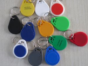 Keyfob
1 Pieces / (Min. Order)
Keyfob
1 Pieces / (Min. Order)
-
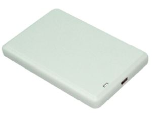 HF Reader
1 Pieces / (Min. Order)
HF Reader
1 Pieces / (Min. Order)
-
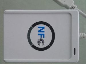 NFC Reader
1 Pieces / (Min. Order)
NFC Reader
1 Pieces / (Min. Order)
-
 UHF Desktop Reader
1 Pieces / (Min. Order)
UHF Desktop Reader
1 Pieces / (Min. Order)
-
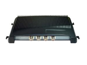 UHF Fixed Reader
1 Pieces / (Min. Order)
UHF Fixed Reader
1 Pieces / (Min. Order)
-
 NFC Small Tag
1 Pieces / (Min. Order)
NFC Small Tag
1 Pieces / (Min. Order)
-
 NFC Sticker
1 Pieces / (Min. Order)
NFC Sticker
1 Pieces / (Min. Order)
-
 Impinj H47
1 Pieces / (Min. Order)
Impinj H47
1 Pieces / (Min. Order)
-
 Impinj-J51
1 Pieces / (Min. Order)
Impinj-J51
1 Pieces / (Min. Order)
-
 Impinj E53
1 Pieces / (Min. Order)
Impinj E53
1 Pieces / (Min. Order)
-
 Impinj E52
1 Pieces / (Min. Order)
Impinj E52
1 Pieces / (Min. Order)
-
 Impinj E42
1 Pieces / (Min. Order)
Impinj E42
1 Pieces / (Min. Order)
-
 Impinj E51
1 Pieces / (Min. Order)
Impinj E51
1 Pieces / (Min. Order)
-
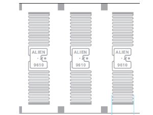 ALIEN 9610
1 Pieces / (Min. Order)
ALIEN 9610
1 Pieces / (Min. Order)
-
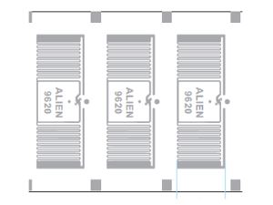 ALIEN 9620
1 Pieces / (Min. Order)
ALIEN 9620
1 Pieces / (Min. Order)
-
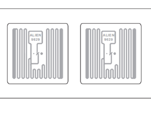 ALIEN 9629
1 Pieces / (Min. Order)
ALIEN 9629
1 Pieces / (Min. Order)
-
 ALIEN 9654
1 Pieces / (Min. Order)
ALIEN 9654
1 Pieces / (Min. Order)
-
 ALIEN 9630
1 Pieces / (Min. Order)
ALIEN 9630
1 Pieces / (Min. Order)
-
 ALIEN 9640
1 Pieces / (Min. Order)
ALIEN 9640
1 Pieces / (Min. Order)
 Frequent updates ensuring high quality data
 Over 5000 customers trust us to help grow their business!

 Menu
Menu