 Menu
Menu


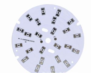
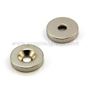
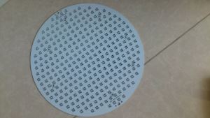
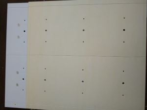
Counter Sink Screw Holes M3 Aluminum LED PCB
-
Min Order
1
-
Product Unit
Pieces
-
Origin
China Mainland
-
Payment


- Contact Now Start Order
- Favorites Share
- Description
Product Detail
![]()
Technical Capabilities
Items | Speci. | Remark | |
Max panel size | 32" x 20.5"(800mm x 520mm) | ||
Min trace width/ space (inner layer) | 4mil/4mil(0.1mm/0.1mm) | ||
Min PAD (inner layer) | 5 mil(0.13mm) | hole ring width | |
Min thickness(inner layer) | 4 mil(0.1mm) | without copper | |
Inner copper thickness | 1~4 oz | ||
Outer copper thickness | 0.5~6 oz | ||
Finished board thickness | 0.4-3.2 mm | ||
| ±0.10 mm | ±0.10 mm | 1~4 L |
±10% | ±10% | 6~8 L | |
±10% | ±10% | =10 L | |
Inner layer treatment | brown oxidation | ||
Layer count Capability | 1-30 LAYER | ||
alignment between ML | ±2mil | ||
Min drilling | 0.15 mm | ||
Min finished hole | 0.1 mm | ||
Hole precision | ±2 mil(±50 um) | ||
tolerance for Slot | ±3 mil(±75 um) | ||
tolerance for PTH | ±3 mil(±75um) | ||
tolerance for NPTH | ±2mil(±50um) | ||
Max Aspect Ratio for PTH | 8:1 | ||
Hole wall copper thickness | 15-50um | ||
Alignment of outer layers | 4mil/4mil | ||
Min trace width/space for outer layer | 4mil/4mil | ||
Tolerance of Etching | +/-10% | ||
Thickness of solder mask | on trace | 0.4-1.2mil(10-30um) | |
at trace corner | =0.2mil(5um) | ||
On base material | =+1.2mil | ||
Hardness of solder mask | 6H | ||
Alignment of solder mask film | ±2mil(+/-50um) | ||
Min width of solder mask bridge | 4mil(100um) | ||
Max hole with solder plug | 0.5mm | ||
Surface finish | HAL (Lead or Lead free), immersion Gold, Immersion Nickel, Electric Gold finger, Electric Gold, OSP, Immersion Silver. | ||
Max Nickel thickness for Gold finger | 280u"(7um) | ||
Max gold thickness for Gold finger | 30u"(0.75um) | ||
Nickel thickness in Immersion Gold | 120u"/240u"(3um/6um) | ||
Gold thickness in Immersion Gold | 2u"/6u"(0.05um/0.15um) | ||
Impedance control and its tolerance | 50±10%,75±10%,100±10% 110±10% | ||
Trace Anti-stripped strength | =61B/in(=107g/mm) | ||
bow and twist | 0.75% | ||
Shenzhen Found has the solution for your printed circuit board thermal management needs. With our knowledge of thermal management and has been certified ISO 9001-2008, ISO 14001-2004 and ISO/TS 16949-2009. we will find the right solution for you whether it is a single sided or multilayer design construction. Found will support you from prototype stage right through to the production of small to large quantities from the far east.
What is a MCPCB? A metal core printed circuit board integrates a heat spreader in the form of a base material- generally aluminum or copper alloy-which is incorporated into the PCB. It achieves a reduced thermal resistance by making use of dielectric polymer prepreg. This provides a transferring heat rate 8-12 times faster than a conventional FR4 PCB.
With a wide range of constructions, Found can support your single sided, 2 layer or multilayer requirements. A wide range of capabilities allows you to add thermal vias, filled vias and blind vias to your design. Our dielectric polymer prepreg materials offer some of the best thermal management properties for LED Lighting, DC-DC power and Military applications. All materials are UL approved with to ensure safety and traceability. For more extreme LED lighting applications contact us about our “Super Pillar” technology. This allows for a thermal conductivity up to 300W/mk and is a unique product only through Found. For bendable or non-rigid MCPCB designs, enquire about our new material able to bend and shape to different angles used for LED lighting.
We understand the need for rapid manufacturing lead times and high quality product. At Found we can support you with fast lead times and ensure you get your boards delivered on-time defect free.
-
Computer-tipped Drill 1 Pieces / (Min. Order)
-
Countersunk Detacher 1 Pieces / (Min. Order)
-
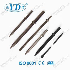
Double Flute SDS Plus Drills 1 Pieces / (Min. Order)
-
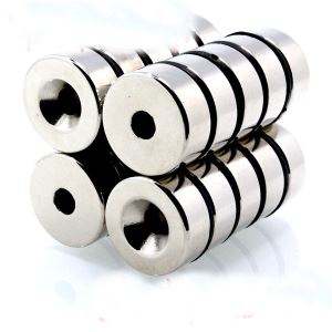
Countersunk Magnets 1 Pieces / (Min. Order)
-
Laird Counter Sink Holes PCB 1 Pieces / (Min. Order)
-
Alloy Steel Casting Drill Bit 1 Pieces / (Min. Order)
-
Countersunk Round Base Cup Magnet 1 Pieces / (Min. Order)
-
Counterweight Crane 1 Pieces / (Min. Order)

-
Print Silk Twilly 1 Pieces / (Min. Order)

-
Coasters For Drinks 1 Pieces / (Min. Order)

-
Crusher Hex Drill Rod 1 Pieces / (Min. Order)
-
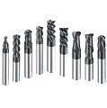
Router End Mills 1 Pieces / (Min. Order)
-
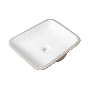
Undercounter Sink, SS-U1612A 1 Pieces / (Min. Order)
-
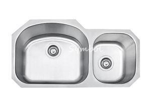
Countertop Sinks, SS-3218AL 1 Pieces / (Min. Order)
 Favorites
-
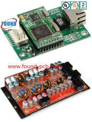 PCBA Board Assembly PCBA Module Fr4 PCBA
1 Pieces / (Min. Order)
PCBA Board Assembly PCBA Module Fr4 PCBA
1 Pieces / (Min. Order)
-
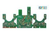 FR4 With Deep Control SLOT Suppliers
1 Pieces / (Min. Order)
FR4 With Deep Control SLOT Suppliers
1 Pieces / (Min. Order)
-
 Rogers 4350B Rogers 4003C PCB
1 Pieces / (Min. Order)
Rogers 4350B Rogers 4003C PCB
1 Pieces / (Min. Order)
-
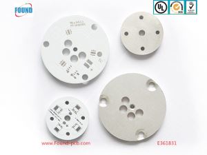 1L MC PCB Count Sink PCB Screw Holes 4.0MM Manufacturers
1 Pieces / (Min. Order)
1L MC PCB Count Sink PCB Screw Holes 4.0MM Manufacturers
1 Pieces / (Min. Order)
-
 CEM-1 CEM-3 FR4 Single Sided Customized PCB
1 Pieces / (Min. Order)
CEM-1 CEM-3 FR4 Single Sided Customized PCB
1 Pieces / (Min. Order)
-
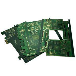
 HDI High Frequency Precision Fr4 PCB Circuit Board RoHS High Frequency Rigid Flex PCB And 94V0 PCB Board
1 Pieces / (Min. Order)
HDI High Frequency Precision Fr4 PCB Circuit Board RoHS High Frequency Rigid Flex PCB And 94V0 PCB Board
1 Pieces / (Min. Order)
-
 Multilayer PCB Circuit Board Rigid-Flex PCB Circuits Board Custom High Quality Rigid-Flex Circuit Board (MIC0490)
1 Pieces / (Min. Order)
Multilayer PCB Circuit Board Rigid-Flex PCB Circuits Board Custom High Quality Rigid-Flex Circuit Board (MIC0490)
1 Pieces / (Min. Order)
-
Laird Counter Sink Holes PCB
1 Pieces / (Min. Order)
-
 Reliable Electronic SMT PCB AssemblyFactory Price ODM/OEM Fr-4 Circuit Board Custom PCB Board PCB Assembly
1 Pieces / (Min. Order)
Reliable Electronic SMT PCB AssemblyFactory Price ODM/OEM Fr-4 Circuit Board Custom PCB Board PCB Assembly
1 Pieces / (Min. Order)
 Frequent updates ensuring high quality data
 Over 5000 customers trust us to help grow their business!


 Menu
Menu