 Menu
Menu


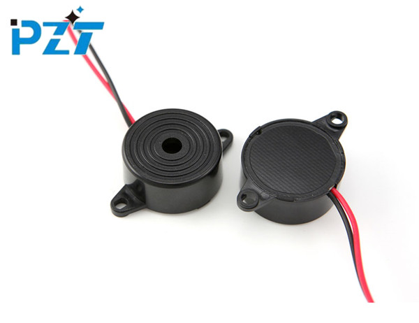
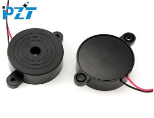
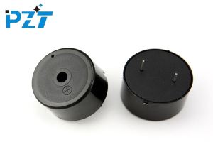
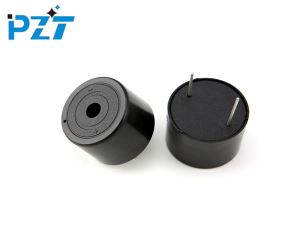
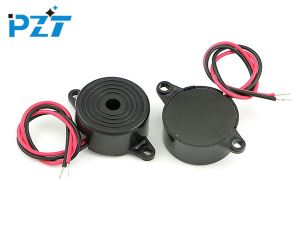
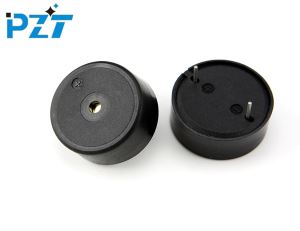
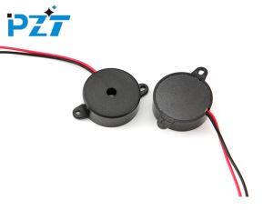
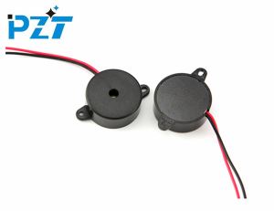
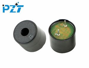
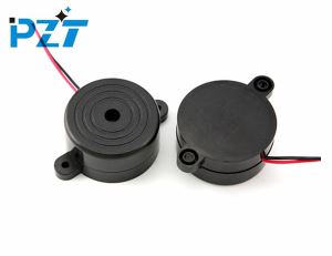
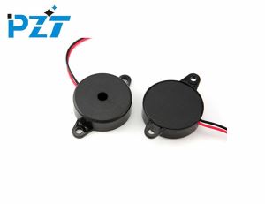
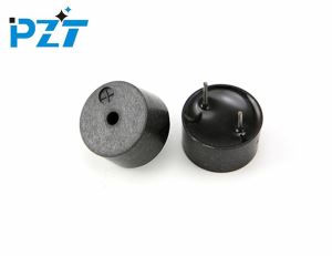
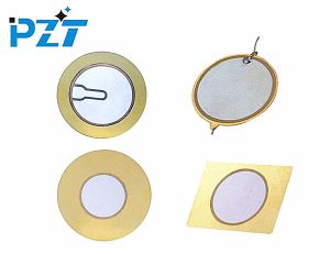
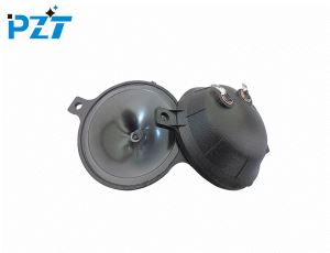
Piezo Beeper
-
Min Order
1
-
Product Unit
Pieces
-
Origin
China Mainland
-
Payment


- Contact Now Start Order
- Favorites Share
- Description
Product Detail
Piezo beeper
Model | LPB2413W1003-TA-12-3.3-R |
Rated Voltage | 12 VDC |
Operating Voltage | 5~30 VDC |
Current Consumption | =15 mA |
Test distance | 10 cm |
SPL | =90 dB @10cm |
Resonant Frequency | 3300±500 Hz |
Tone | Continuous sound |
Operating Temperature | -20 ~ +70 ? |
Storage Temperature | -30 ~ +80 ? |
Weight | 3 g |
Carton size | 66×36×29 cm |
Quantity | 2000 pcs |
Gross Weight | 8 Kg |
Microcontroller-driven piezoelectric buzzer improvements
This article focuses on how to use a microcontroller to drive a piezo buzzer at a large AC voltage, using a four-MOSFET circuit that interfaces with the microcontroller's two I / O pins (Reference 1). The following is a modification of this circuit expansion, saving the I / O pin of the next microcontroller. The gate of Q4 is connected to the drain of Q2 instead of the second I / O pin (Figure). The microprocessor applies a high logic level to the I / O pin, turning Q2 on and pulling Node A low. This action opens Q3 and closes Q4. The voltage on Node B becomes 15V and Q1 turns off. The voltage on the piezo element is now 15V.

A microcontroller I / O pin drives this circuit, producing an AC voltage across the piezo buzzer
The microcontroller then switches the I / O pin low and Q2 turns off. Q1 is also off, so Node A slowly ramps to a high logic level by pulling the resistor R1. When the voltage on Node A reaches the inverter switching threshold formed by the pair of Q3 and Q4 tubes, Q3 turns off rapidly and Q4 turns on quickly. As a result, the low logic level on Node B turns on Q1 and speeds up the voltage on NodeA. Now, the 15V voltage on the piezo buzzer is the opposite polarity.
R2 weakens the coupling between the Q4 output and the input because of the presence of the piezo element. The R2 value of 330O is usually enough to suppress high frequency oscillations caused by feedback. If the R1 resistance is small, it will increase the power drawn from the power supply. R1 value is too large will increase the power consumption, because it will extend the transistor switching time, increase the relevant through-current. The optimal value of R1 is about 1kO.
This design saves an I / O pin, but at the expense of increased power consumption. Therefore, the power consumption of the circuit than the previous design example described an order of magnitude higher.
-
Photocoupler YKA2404S 1 Pieces / (Min. Order)
-
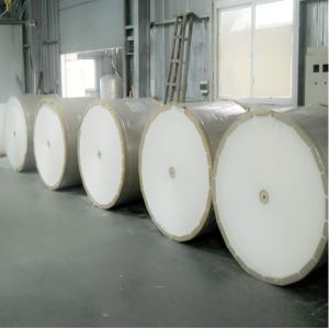
PE Coated Paper Roll 1 Pieces / (Min. Order)

-
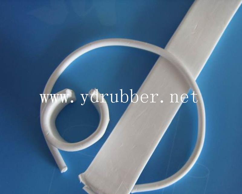
PTFE Tape 1 Pieces / (Min. Order)

-
Bottom Paper 1 Pieces / (Min. Order)

-
PE Coated Paper Roll 1 Pieces / (Min. Order)
-
PTFE Tape 1 Pieces / (Min. Order)
-
PE Coated Cup Paper 1 Pieces / (Min. Order)
-
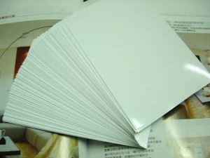
Photo Copy Paper 1 Pieces / (Min. Order)
-
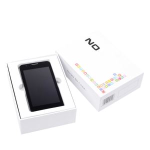
Phone Paper Box 1 Pieces / (Min. Order)
 Favorites
-
 Piezo Alarm Buzzer
1 Pieces / (Min. Order)
Piezo Alarm Buzzer
1 Pieces / (Min. Order)
-
 12 Volt Piezo Buzzer
1 Pieces / (Min. Order)
12 Volt Piezo Buzzer
1 Pieces / (Min. Order)
-
 Piezoelectric Sounder
1 Pieces / (Min. Order)
Piezoelectric Sounder
1 Pieces / (Min. Order)
-
 Piezo Buzzer With Wire Lead
1 Pieces / (Min. Order)
Piezo Buzzer With Wire Lead
1 Pieces / (Min. Order)
-
 23mm Piezo Buzzer
1 Pieces / (Min. Order)
23mm Piezo Buzzer
1 Pieces / (Min. Order)
-
 12v Buzzer Tweeter
1 Pieces / (Min. Order)
12v Buzzer Tweeter
1 Pieces / (Min. Order)
-
 24v Piezo Buzzer
1 Pieces / (Min. Order)
24v Piezo Buzzer
1 Pieces / (Min. Order)
-
 Piezo Sounder
1 Pieces / (Min. Order)
Piezo Sounder
1 Pieces / (Min. Order)
-
 Piezo Alarm
1 Pieces / (Min. Order)
Piezo Alarm
1 Pieces / (Min. Order)
-
 Piezoelectric Buzzer
1 Pieces / (Min. Order)
Piezoelectric Buzzer
1 Pieces / (Min. Order)
-
 12v Piezo Buzzer
1 Pieces / (Min. Order)
12v Piezo Buzzer
1 Pieces / (Min. Order)
-
 Piezo Disk
1 Pieces / (Min. Order)
Piezo Disk
1 Pieces / (Min. Order)
-
 Piezo Tweeter
1 Pieces / (Min. Order)
Piezo Tweeter
1 Pieces / (Min. Order)
-
 Piezo Atomizer Disc
1 Pieces / (Min. Order)
Piezo Atomizer Disc
1 Pieces / (Min. Order)
-
 Piezo Bender 27mm
1 Pieces / (Min. Order)
Piezo Bender 27mm
1 Pieces / (Min. Order)
 Frequent updates ensuring high quality data
 Over 5000 customers trust us to help grow their business!


 Menu
Menu