 Menu
Menu


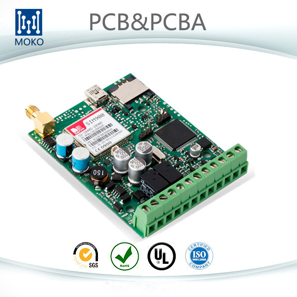
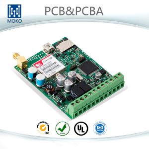


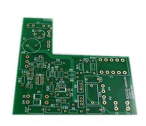
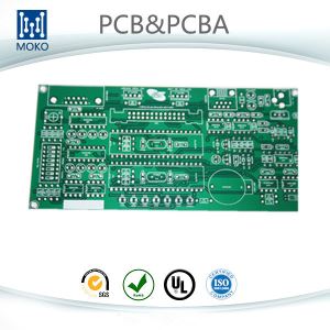
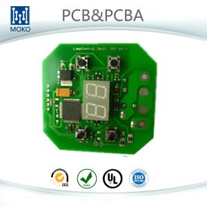
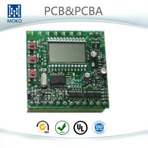
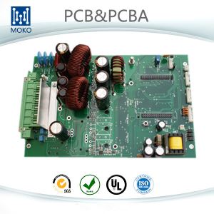
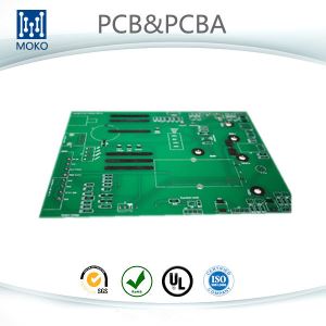
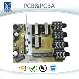
Customized Sim908 GPS Tracking Board ,GPS Tracker PCBA In Shenzhen
-
Min Order
1
-
Product Unit
Pieces
-
Origin
China Mainland
-
Payment


- Contact Now Start Order
- Favorites Share
- Description
Product Detail
Quick Details
Place of Origin: Guangdong, China (Mainland)
Brand Name: Moko
Model Number: MK50806BJ02
Number of Layers: 2 Layer
Base Material: FR4 ,Aluminum,PI
Copper Thickness: 1oz
Board Thickness: 1.6mm
Min. Hole Size: 0.25mm
Min. Line Width: 0.1mm
Min. Line Spacing: 0.1mm
Surface Finishing: HASL,Nickle,Immersion Gold,Immersion Tin
Standard: IPC-A-610D
Wrap and twist: =0.5%
V-Score Depth: 20-25% of board thickness
Design File Formate: Gerber RS-274,274D,Eagle and AutoCAD's DXF,DWG
Solder mask color: Green,Blue,Black,White,Red,Yellow
PCB Special technique: Blind&buried via,Impedance control
Certificate: UL, ISO 9001, ISO 14001, ROHS
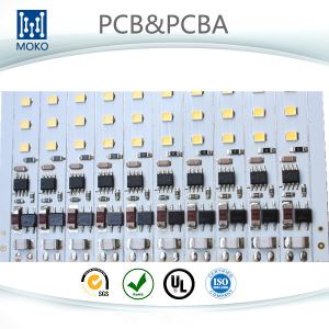
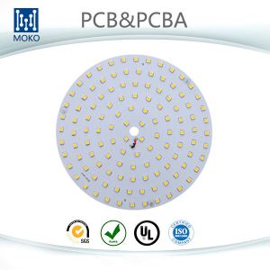
Specialised in: LED,medical,industrial boards
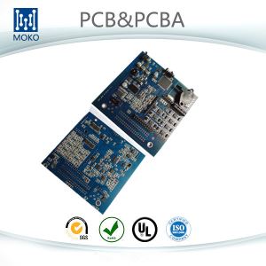
Service: PCB,Turnkey PCBA,PCB clone,Comp
Packaging & Delivery
| Packaging Details: | Inner packing :Vacuum Package Outer packing:Standard Carton |
|---|---|
| Delivery Detail: | PCB:5-7 days ;PCBA:15-20 days |
PCB Technical Specification
| Number of Layer | 1,2,4 or 6,upto 18 layer |
| Order Quantity | 1 to 50,000 |
| Board Shape | Retangular,round,slots,cutouts,complex,irregular |
| Board Type | Rigid, Flexible, Rigid-flexible |
| Board Material | FR-4 glass epoxy, FR-4 high Tg, Rohs compliant,Aluminum,Rogers,etc. |
| Board Cutting | Shear,V-score,Tab-routed |
| Board Thickness | 0.2-4.0mm, Flex 0.01-0.25mm |
| Copper Weight | 1.0, 1.5, 2.0 oz |
| Solder Mask | Double-sided green LPI,Also support Red,White,Yellow,Blue,Black |
| Silk Screen | Double-sided or single-sided in white,yellow,black,or negative |
| Silk Screen Min Line Width | 0.006'' or 0.15mm |
| Max Board Dimensions | 20 inch*20inch or 500mm*500mm |
| Min Trace/Gap | 0.10mm, or 4mils |
| Min Drill Hole Diameter | 0.01'',0.25mm, or 10mils |
| Surface Finish | HASL,Nickle,Immersion Gold,Immersion Tin,Immersion Silver,OSP,etc. |
| Board Thickness Tolerance | ±10% |
| Copper Weight Tolerance | ± 0.25 oz |
| Minimal Slot Width | 0.12'', 3.0mm, or 120mils |
| V-Score Depth | 20-25% of board thickness |
| Design File Formate | Gerber RS-274,274D,Eagle and AutoCAD's DXF,DWG |
PCBA Capabilities
| Quantity | Prototype&Low Volume PCB Assembly,from 1 Board to 250,is specialty,or up to 1000 |
| Type of Assembly | SMT,Thru-hole |
| Solder Type | Water Soluble Solder Paste,Leaded and Lead-Free |
| Components |
Passive Down to 0201 size |
| Bare Board Size |
Smallest:0.25*0.25 inches |
| File Formate |
Bill of Materials |
| Types of Service | Turn-key,partial turn-key or consignment |
| Component packaging | Cut Tape,Tube,Reels,Loose Parts |
| Turn Time | Same day service to 15 days service |
| Testing | Flying Probe Test,X-ray Inspection AOI Test |
| PCB assembly process |
Drilling-----Exposure-----Plating-----Etaching & Stripping-----Punching-----Electrical Testing-----SMT-----Wave Soldering-----Assembling-----ICT-----Function Testing-----Temperature & Humidity Testing |
PCB Lead time:
| Single/double side | 4 layer | 6 layer | Above 8 layer | HDI | |
| Sample lead time(Normal) | 5-6 | 6-7 | 7-8 | 10-12 | 15-20 |
| Sample lead time(Fastest) | 48-72 hours | 5 | 6 | 6-7 | 12 |
| Mass production lead time(First batch) | 7-9 | 10-12 | 13-15 | 16 | 20 |
-
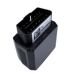
Car Tracking Device OBD GPS Tracker OBDII Vehicle Tracker VT100 1 Pieces / (Min. Order)
-
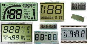
Digital Display COG COB display graphic OLED display oled suppliers customerized LCD display 1 Pieces / (Min. Order)
-
Custom glod foil embossed box security seal stickers, glod foil stamped security tamper 1 Pieces / (Min. Order)
-
Quartz Engineered Stones color chart with free silestone samples 1 Pieces / (Min. Order)
-
RAC 5 Paint Airless Spray Black Tips Accessoires 1 Pieces / (Min. Order)

-
Prink Printed Polyester 600D Backpack With Zipper Pocket 1 Pieces / (Min. Order)
-
Casting Iron Front Wheel Hub Cast Iron Accessories 1 Pieces / (Min. Order)
-
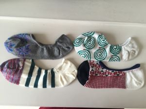
Jacquard And Solid No Show Socks For Ladies Low-Cut Boat Shoes 1 Pieces / (Min. Order)
-
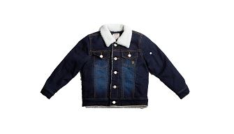
Customized Boys Girls Men Snowboard Sport Jackets Ski Jacket Moto Monogrammed Jacket 1 Pieces / (Min. Order)
-
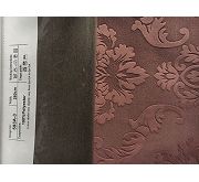
280cm Curtain Velvet Fabric Blackout Plain Dyeing Embossed Burnout Brushed 1 Pieces / (Min. Order)
-
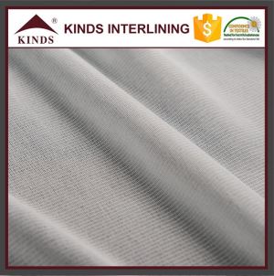
High Quality Polyester Tricot Knitted Interlining 1 Pieces / (Min. Order)
-
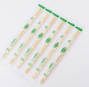
Customized Round Bamboo Chopsticks With Logo Printed 1 Pieces / (Min. Order)
-
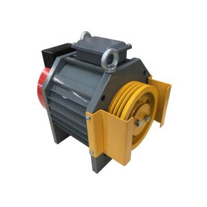
Elevator Gearless Traction Drive KA320C Series 1 Pieces / (Min. Order)
-
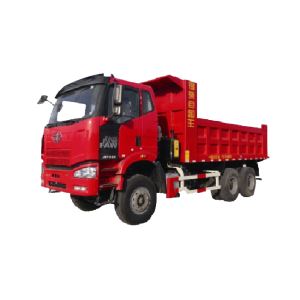
Best Small Tandem Axle Dump Truck Sales Prices 1 Pieces / (Min. Order)
-
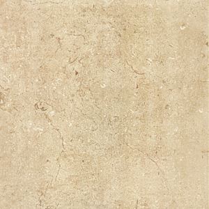
Porcelain Floor Tile Ceramic Tiles Glazed Tiles Outdoor Used Tiles 1 Pieces / (Min. Order)
-
Corrugated Cardboard Tray Display For Accessories 1 Pieces / (Min. Order)
 Favorites
-
 Protel PCB Supplier, Protel Printed Circuit Boards
1 Pieces / (Min. Order)
Protel PCB Supplier, Protel Printed Circuit Boards
1 Pieces / (Min. Order)
-
 Telecom Communication PCB Manufacturer, Telecom PCB Boards
1 Pieces / (Min. Order)
Telecom Communication PCB Manufacturer, Telecom PCB Boards
1 Pieces / (Min. Order)
-
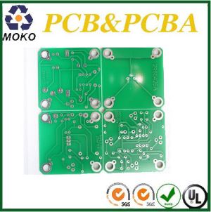 Printed Circuit Boards Production
1 Pieces / (Min. Order)
Printed Circuit Boards Production
1 Pieces / (Min. Order)
-
 Bare Board Electrical Testing Capabilities
1 Pieces / (Min. Order)
Bare Board Electrical Testing Capabilities
1 Pieces / (Min. Order)
-
 Medical PCB Assembly, Medical PCB Prototype
1 Pieces / (Min. Order)
Medical PCB Assembly, Medical PCB Prototype
1 Pieces / (Min. Order)
-
 Customized Remote Control Transmitter And Receiver PCBA Circuit
1 Pieces / (Min. Order)
Customized Remote Control Transmitter And Receiver PCBA Circuit
1 Pieces / (Min. Order)
-
 Digital FM Receiver Circuit Board Assembly Production
1 Pieces / (Min. Order)
Digital FM Receiver Circuit Board Assembly Production
1 Pieces / (Min. Order)
-
 Customized Audio Amplifier Circuit For Cars
1 Pieces / (Min. Order)
Customized Audio Amplifier Circuit For Cars
1 Pieces / (Min. Order)
-
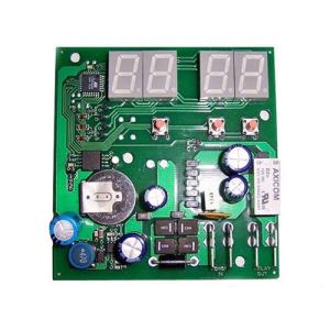
 Quality Assured LED Display Circuit Board Assembly
1 Pieces / (Min. Order)
Quality Assured LED Display Circuit Board Assembly
1 Pieces / (Min. Order)
-
 Powered LED Road Traffic Sign PCBA Board
1 Pieces / (Min. Order)
Powered LED Road Traffic Sign PCBA Board
1 Pieces / (Min. Order)
-
 Outdoor LED Advertising PCB Board With Electronic Components Placed
1 Pieces / (Min. Order)
Outdoor LED Advertising PCB Board With Electronic Components Placed
1 Pieces / (Min. Order)
-
 Rigid LCD Display PCB Assembly Board
1 Pieces / (Min. Order)
Rigid LCD Display PCB Assembly Board
1 Pieces / (Min. Order)
-
 One Stop OEM GPS Tracking System PCBA Supplier ,Electronic Board
1 Pieces / (Min. Order)
One Stop OEM GPS Tracking System PCBA Supplier ,Electronic Board
1 Pieces / (Min. Order)
-
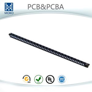
 AssembLED LED Board PCB
1 Pieces / (Min. Order)
AssembLED LED Board PCB
1 Pieces / (Min. Order)
-
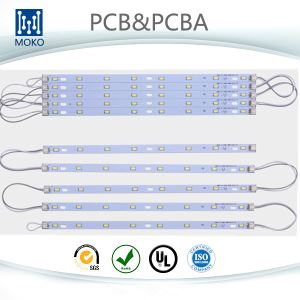
 Energy Saving LED Lamp Assemble Service, RoHS Qualified Circuit Card For LED
1 Pieces / (Min. Order)
Energy Saving LED Lamp Assemble Service, RoHS Qualified Circuit Card For LED
1 Pieces / (Min. Order)
-
 Electronic Circuits Board Assembly PCB Circuit Board Assembly
1 Pieces / (Min. Order)
Electronic Circuits Board Assembly PCB Circuit Board Assembly
1 Pieces / (Min. Order)
-
 PCB Circuit Assembly For Industrial Control
1 Pieces / (Min. Order)
PCB Circuit Assembly For Industrial Control
1 Pieces / (Min. Order)
-
 High Thick Copper PCB Power Board
1 Pieces / (Min. Order)
High Thick Copper PCB Power Board
1 Pieces / (Min. Order)
-
 Power Supply PCB Circuit Board Partern
1 Pieces / (Min. Order)
Power Supply PCB Circuit Board Partern
1 Pieces / (Min. Order)
 Frequent updates ensuring high quality data
 Over 5000 customers trust us to help grow their business!

 Menu
Menu