 Menu
Menu


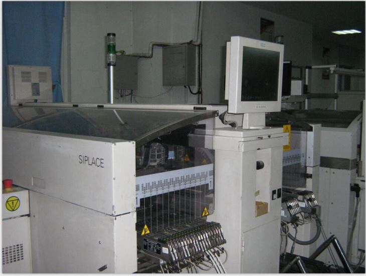

Automated Optical Inspection
-
Min Order
1
-
Product Unit
Pieces
-
Origin
China Mainland
-
Payment


- Contact Now Start Order
- Favorites Share
- Description
Product Detail
Automatic Optic Inspection
The full name of AOI (Automatic Optic Inspection) is automatic optical inspection. It is a device based on the optical principle to detect common defects encountered in welding production. AOI is a new type of test technology that has emerged, but it has developed rapidly. Many manufacturers have introduced AOI test equipment. When automatically detected, the machine automatically scans the PCB through the camera, collects images, and compares the tested solder joints with the qualified parameters in the database. After image processing, the defects on the PCB are detected, and the defects are displayed/marked through the display or the automatic mark. Come out for maintenance personnel to trim.
Area of interest The name of the study area in some software for remote sensing and GIS. Use high-speed and high-precision visual processing technology to automatically detect various mis-installation errors and welding defects on the PCB. PCB boards range from fine-pitch high-density boards to low-density large-size boards, and provide on-line inspection solutions to increase production efficiency and weld quality. By using AOI as a tool to reduce defects, errors are found and eliminated early in the assembly process to achieve good process control. Early detection of defects will avoid the delivery of bad boards to the subsequent assembly stage, and AOI will reduce repair costs to avoid scrapping unrepairable circuit boards.
Features
1) High-speed detection system
Has nothing to do with the density of PCB board affixing
2) Fast and convenient programming system
Under the graphical interface
Automatic detection of data using post data
Use component database for rapid editing of test data
3) Use rich special multi-function detection algorithms and binary or gray level optical imaging processing technology to detect
4) Automatically correct the detection window according to the momentary change of the position of the detected component to achieve high-precision detection
5) Detecting the electrical power by marking directly on the PCB with ink or using graphic error indication on the operation display
Attributes and Capabilities of AOI Test
Depending on visual methods, AOI test can be applied to detect a lot of surface defects including scratches, nodules, stains, opens, shorts, insufficient or excessive solder, incorrect components, missing components, incorrect polarity of components etc. As a matter of fact, these defects AOI is capable of going through belong to items of manual visual inspection that was mainly applied prior to the popularity of AOI test which is, however, capable of performing them quickly and accurately.
• Multiple inspection objects - AOI test works perfectly for both bare PCBs and PCBAs. For PCB inspection, defects are checked such as shorts, opens and insufficient solder. For PCBA inspection, issues are inspected including component soldering, polarity and values.
• Flexibility - Automated Optical Inspection can be arranged in any stage of manufacturing line in accordance customers' needs and cost tolerance capacity. In order to increase inspection efficiency and reduce corresponding cost, it's optimal to place it after reflow soldering because most defects result from nonconformance occurring during soldering process. The flexibility attribute of AOI test leads to reduction of cost since it is an in-process test and as soon as issues are discovered, manufacturing or assembly parameters can be instantly modified so that later products will be correctly produced. As a result, more products won't be rejected during functional test or final inspection.
• Low cost - Compared with Automated/Automatic X-ray Inspection (AXI), post-reflow AOI is less expensive when it comes to solder joint defects inspection including bridges, broken joints, dry joints etc.
• Accuracy and Reliability
Working Principle of AOI Test
AOI test achieves its inspection process by scanning board surface. Depending on one or more high-definition cameras, this equipment can capture images of PCB surface with the help of numerous light sources including fluorescent lighting, LED lighting or infra-red or ultra-violet lighting. Then, comparison will be made between the captured image and board parameters that have been input into computer in advance so that differences, abnormalities or even errors can be clearly indicated by its built-in processing software. The whole process can be monitored at any second.
The analysis whether a board is perfect or features issues can be drawn by different algorithms applied by AOI. When it comes to simple applications inspection, pixel-counting algorithm is used containing the following methods.
• Template matching - Template-matching method, also called area-based method or correlation-like method, has been popular for a couple of decades. Based on pixel-by-pixel method, a small template is applied to a large inspection image through sliding template window. Then, normalized cross correlation (NCC) will be calculated between the template and inspection image. The larger the value of NCC is, the higher matching between them will be.
• Object recognition - Object recognition conforms to the same principle as view method in that difference is observed through comparison between an ideal image and the captured image of an object.
• Blob analysis - Blob analysis refers to a process during which the object is separated from the background first. Then with a pixel-based image applied, a blob is generated through grouping of object pixels to inspect issues of objects.
Owing to the progress of technologies and higher demand from market for efficiency and effectiveness, some new methods start to play a major role in PCB or PCBA inspection, among which vectoral imaging technology stands out.
As a pattern location search technology, vectoral imaging is based on geometric feature extraction instead of complete grey scale pixel values. Under such circumstances, the image analysis is not influenced by color changes or non-liner changes. Furthermore, vectoral imaging performs better in reduction of false failures due to the attribute of background elimination.
AOI Test from JIA-SPEED
As a primary testing technique in PCB assembly, AOI applies to fast and accurate inspection of errors or defects occurring in PCB assembly process so that high quality of PCB assemblies can be ensured with no defects after their leaving assembly line. AOI can be applied both to bare PCBs and PCB assembly.
-
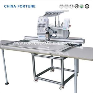
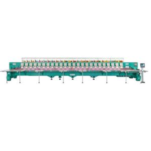
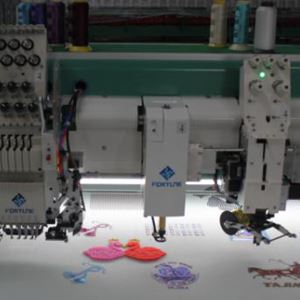
CT1201S Single Head Embroidery Machine Business Box Small Embroidery Machine 1 Pieces / (Min. Order)
-
CT1201 Single Head Embroidery Machine High Quality Logo Pattern F1201m Embroidery Machine 1 Pieces / (Min. Order)
-
CT1201L Single Head Embroidery Machine Free Design Font Pattern 1 Pieces / (Min. Order)
-
CT1201XL Single Head Embroidery Machine Applique Letter Pattern Embroidery Monogramming 1 Pieces / (Min. Order)

-
CT1201xxl Single Head Embroidery Machine Design of Large Domestic Singers 1 Pieces / (Min. Order)
-
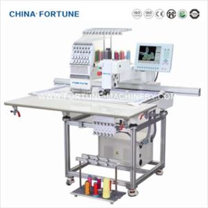
CT1201 + 1pd Single Head Embroidery Machine Custom Multi Needle Business 1 Pieces / (Min. Order)
-
601CT Single Head Embroidery Machine Using Digital Pattern 1 Pieces / (Min. Order)
-
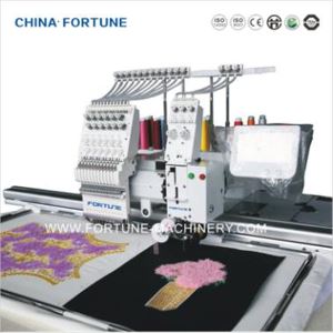
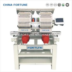
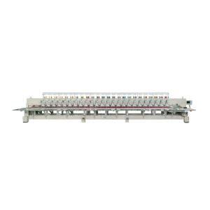
CT1202 Cap Embroidery Machine Letter Combination of Different Kits of 6 Needle Commercial Sewing Embroidery 1 Pieces / (Min. Order)
-
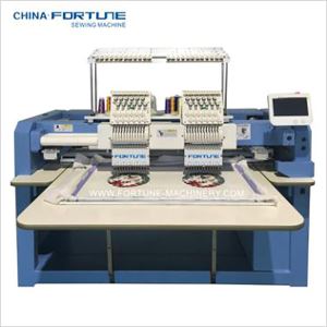
CT1202H Double Head Cap Embroidery Machine Professional Custom Machine 1 Pieces / (Min. Order)
-
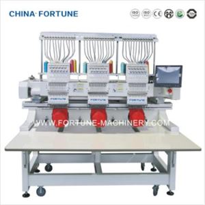
CT1203h Three Head Cap T-shirt Embroidery Machine Best Design Printing 1 Pieces / (Min. Order)
-
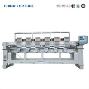
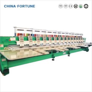
CT906 Six Head Cap T-shirt Embroidery Machine Printing Professional Custom 1 Pieces / (Min. Order)
-
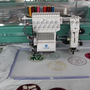
EFG915 Flat Machine Embroidery Clothes Pattern Design Logo Design 1 Pieces / (Min. Order)
-
HFG924 High Speed Machine Quality Blackwork Guarantee Bunka Pattern Embroidery 1 Pieces / (Min. Order)
-
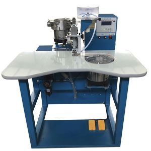
Sequins and Rope Embroidery Machine Combined With Different Patterns 1 Pieces / (Min. Order)
-
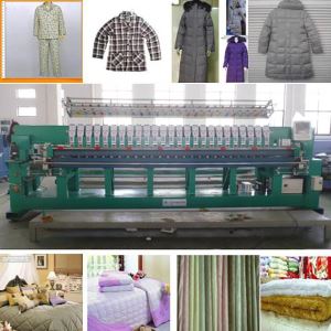
Dribbling Embroidery Machine Lightweight Design Exquisite Pattern Quilt 1 Pieces / (Min. Order)
-
Laser Embroidery Machine Cutting Marking 1 Pieces / (Min. Order)

-
Computer Quilting Embroidery Machine Best Design Free 1 Pieces / (Min. Order)
-
Beaded Embroidery Machine Different Pattern Bag 1 Pieces / (Min. Order)

-
Mixed Function Embroidery Machine Suitable for Flat and Chenille Sequins Dribbling 1 Pieces / (Min. Order)
-
Pearl Sewing Machine with Repair Bead Piece 1 Pieces / (Min. Order)
 Favorites
-
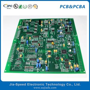 SMT Through Hole Electronic PCB Circuit Board Assembly
1 Pieces / (Min. Order)
SMT Through Hole Electronic PCB Circuit Board Assembly
1 Pieces / (Min. Order)
-
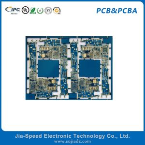 Immersion Gold Pcb Multilayer Circuit Board With Blue Solder Mask
1 Pieces / (Min. Order)
Immersion Gold Pcb Multilayer Circuit Board With Blue Solder Mask
1 Pieces / (Min. Order)
-
Immersion Gold Pcb Multilayer Circuit Board With Blue Solder Mask
1 Pieces / (Min. Order)
-
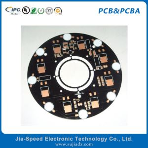 Black Solder Mask Round LED PCB Board
1 Pieces / (Min. Order)
Black Solder Mask Round LED PCB Board
1 Pieces / (Min. Order)
-
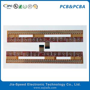 4 layer Flexible PCB / FPC Assembly
1 Pieces / (Min. Order)
4 layer Flexible PCB / FPC Assembly
1 Pieces / (Min. Order)
 Frequent updates ensuring high quality data
 Over 5000 customers trust us to help grow their business!

 Menu
Menu