 Menu
Menu


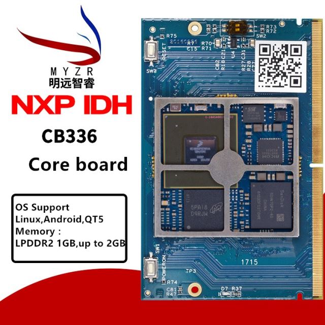
Atmel Core Module
-
Min Order
1
-
Product Unit
Pieces
-
Origin
China Mainland
-
Payment


- Contact Now Start Order
- Favorites Share
- Description
Product Detail
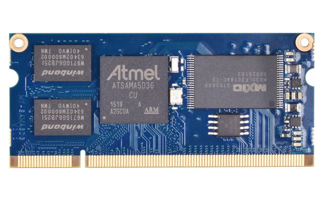
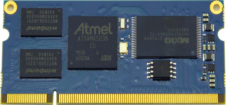
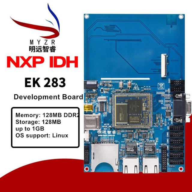
Model: MY-SAMA5-CB200-5D36
Atmel® | SMART SAMA5
ARM Cortex-A5
536MHz (850DMIPS)
256MB DDR3 (64 Bit)
256MB Nandflash, up to 1G
Industrial grade
-40° to 85° C Temp
Top view)
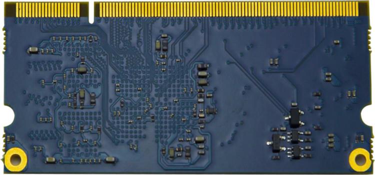
Rear view
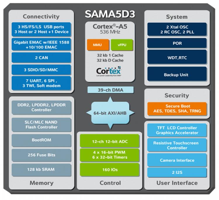
SAMA5D3 diagram
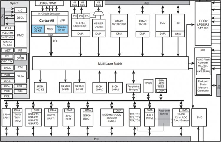
SAMA5D3 block diagram
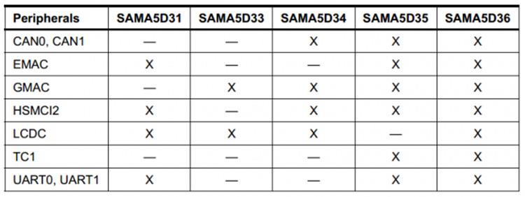
SAMA5D3 MPU difference
SAMA5D36 critical parameter
| Parameter | Value |
| Pin Count: | 324 |
| Max. Operating Freq. (MHz): | 536 MHz |
| CPU: | Cortex-A5 |
| Max I/O Pins: | 160 |
| Ext Interrupts: | 160 |
| USB Transceiver: | 3 |
| USB Speed: | Hi-Speed |
| USB Interface: | Host, Device |
| SPI: | 6 |
| TWI (I2C): | 3 |
| UART: | 7 |
| CAN: | 2 |
| LIN: | 4 |
| SSC: | 2 |
| Ethernet: | 2 |
| SD / eMMC: | 3 |
| Graphic LCD: | Yes |
| Camera Interface: | Yes |
| ADC Channels: | 12 |
| ADC Resolution (bits): | 12 |
| ADC Speed (ksps): | 1000 |
| Resistive Touch Screen: | Yes |
| Crypto Engine: | AES/DES/SHA/TRNG |
| SRAM (Kbytes): | 128 |
| External Bus Interface: | 1 |
| DRAM Memory: | DDR2/LPDDR/LPDDR2 |
| NAND Interface: | Yes |
| Temp. Range (deg C): | -40 to 105 |
| I/O Supply Class: | 1.8/3.3 |
| Operating Voltage (Vcc): | 1.08 to 1.32 |
| FPU: | Yes |
| Timers: | 6 |
| Output Compare Channels: | 6 |
| Input Capture Channels: | 6 |
| PWM Channels: | 4 |
| 32kHz RTC: | Yes |
| MPU / MMU: | No / Yes |
| Quadrature Decoder Channels: | 0 |
| Video Decoder: | No |
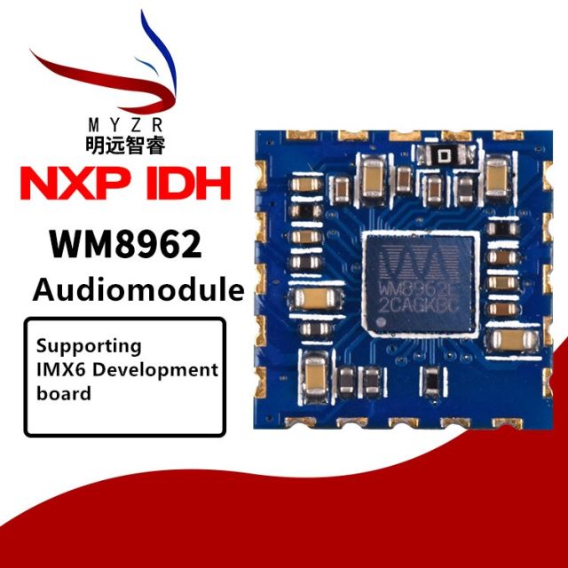
MY-IMX6-CB200 configuration
hardware configuration
CPU | SAMA5D3x | industrial/expansion |
memory | 256MB | up to 512MB |
storage | 256MB | support up to 2GB |
SPI Flash | 2M | support programming |
boot mode | SPI boot | ensure the stability and reliability of products |
working temperature range
Industrial grade: -40°C ~ 85°C
Industrial expansion grade: -40°C ~ 105°C
operation system support
kernel: Linux-3.18
interface:command line
model command
name of model
MY-SAMA5-CB200-MPU specification-memory capacity-storage capacity
MPU specification
D36ACN, D36ACNR:industrial expansion
D36ACU, D36ACUR: industrial
memory capacity
256MB: 256G memory
storage capacity
256MB: 256G storage
example of model
MY-SAMA5-CB200-D36ACN-256M-256M
MY-SAMA5-CB200 definition
| No. | Pin | Default signal | Default Interface | Multiplex | Multiplex | Default Interface | Default signal | Pin | No. |
| 1 | GND_POWER | GND_POWER | 2 | ||||||
| 3 | PC1 | ETX1 | EMAC | TIOB3 | LCDDAT19 | MCI2 | MCI2_DA0 | PC11 | 4 |
| 5 | PC8 | EMDC | TCLK5 | LCDDAT18|TIOA1 | MCI2_DA1 | PC12 | 6 | ||
| 7 | PC3 | ERX1 | TIOA4 | LCDDAT21|PCK2 | MCI2_CK | PC15 | 8 | ||
| 9 | PC6 | ERXER | TIOA5 | LCDDAT17|TIOB1 | MCI2_DA2 | PC13 | 10 | ||
| 11 | PC4 | ETXEN | TIOB4 | LCDDAT20 | MCI2_CDA | PC10 | 12 | ||
| 13 | PC7 | EREFCK | TIOB5 | LCDDAT16|TCLK1 | MCI2_DA3 | PC14 | 14 | ||
| 15 | PC0 | ETX0 | TIOA3 | SSC0 | RK0 | PC19 | 16 | ||
| 17 | PC2 | ERX0 | TCLK3 | TF0 | PC17 | 18 | |||
| 19 | PC5 | ECRSDV | TCLK4 | RF0 | PC20 | 20 | |||
| 21 | PC9 | EMDIO | RD0 | PC21 | 22 | ||||
| 23 | PC30 | UTXD0 | UART0 | ISI_PCK | TK0 | PC16 | 24 | ||
| 25 | PC29 | URXD0 | ISI_D8|PWMFI2 | TD0 | PC18 | 26 | |||
| 27 | GND_POWER | GND_POWER | 28 | ||||||
| 29 | PC31 | PWMFI1|FIQ | LCDC | LCDVSYNC | PA26 | 30 | |||
| 31 | PC23 | SPI1_MOSI | SPI1 | LCDDISP | PA25 | 32 | |||
| 33 | PC25 | SPI1_NPCS0 | GND_POWER | 34 | |||||
| 35 | PC22 | SPI1_MISO | LCDC | LCDHSYNC | PA27 | 36 | |||
| 37 | PC24 | SPI1_SPCK | GND_POWER | 38 | |||||
| 39 | PC28 | SPI1_NPCS3 | ISI_D9|PWMFI0 | LCDC | LCDDEN | PA29 | 40 | ||
| 41 | PA4 | LCDDAT4 | LCDC | LCDDAT2 | PA2 | 42 | |||
| 43 | PA10 | LCDDAT10 | LCDDAT15 | PA15 | 44 | ||||
| 45 | PA14 | LCDDAT14 | ISI_D1 | LCDDAT17 | PA17 | 46 | |||
| 47 | PA12 | LCDDAT12 | LCDDAT1 | PA1 | 48 | ||||
| 49 | PA24 | LCDPWM | LCDDAT0 | PA0 | 50 | ||||
| 51 | PA22 | LCDDAT22 | ISI_D6|PWMH1 | LCDDAT3 | PA3 | 52 | |||
| 53 | PA28 | LCDPCK | LCDDAT8 | PA8 | 54 | ||||
| 55 | PA20 | LCDDAT20 | ISI_D4|PWMH0 | LCDDAT6 | PA6 | 56 | |||
| 57 | PA21 | LCDDAT21 | ISI_D5|PWML0 | ISI_D2|TWD2 | LCDDAT18 | PA18 | 58 | ||
| 59 | PA23 | LCDDAT23 | ISI_D7|PWML1 | ISI_D0 | LCDDAT16 | PA16 | 60 | ||
| 61 | PA5 | LCDDAT5 | ISI_D3|TWCK2 | LCDDAT19 | PA19 | 62 | |||
| 63 | PA7 | LCDDAT7 | LCDDAT11 | PA11 | 64 | ||||
| 65 | PA30 | TWD0 | TWI0 | URXD1|ISI_VSYNC | LCDDAT9 | PA9 | 66 | ||
| 67 | PA31 | TWCK0 | UTXD1|ISI_HSYNC | LCDDAT13 | PA13 | 68 | |||
| 69 | PD31 | PCK1|AD11 | ISI_D10|SPI1_NPCS2 | TWI1 | TWCK1 | PC27 | 70 | ||
| 71 | PD30 | PCK0 | SSC0:CLK | AD10 | ISI_D11|SPI1_NPCS1 | TWD1 | PC26 | 72 | |
| 73 | PD29 | AD9 | AD | MCI0 | MCI0_DA3 | PD4 | 74 | ||
| 75 | PD28 | AD8 | MCI0_DA1 | PD2 | 76 | ||||
| 77 | PD27 | AD7 | MCI0_CDA | PD0 | 78 | ||||
| 79 | PD26 | AD6 | MCI0_CK | PD9 | 80 | ||||
| 81 | PD23 | AD3 | MCI0_DA2 | PD3 | 82 | ||||
| 83 | PD22 | AD2 | MCI0_DA0 | PD1 | 84 | ||||
| 85 | PD24 | AD4 | PWML2|TIOB0 | MCI0_DA5 | PD6 | 86 | |||
| 87 | PD21 | AD1 | PWML3 | MCI0_DA7 | PD8 | 88 | |||
| 89 | PD25 | AD5 | SPI0_NPCS2|CTS0 | CAN0 | CANTX0 | PD15 | 90 | ||
| 91 | PD20 | AD0 | SPI0_NPCS1|SCK0 | CANRX0 | PD14 | 92 | |||
| 93 | PD5 | PWMH2 | PWM | MCI0_DA4|TIOA0 | UART0 | TXD0 | PD18 | 94 | |
| 95 | PD7 | PWMH3 | MCI0_DA6|TCLK0 | RXD0 | PD17 | 96 | |||
| 97 | PD19 | GPIO | ADTRG | SPI0 | SPI0_MISO | PD10 | 98 | ||
| 99 | PB0 | GTX0 | GMAC | PWMH0 | SPI0_SPCK | PD12 | 100 | ||
| 101 | PB7 | GRX3 | RK1 | SPI0_MOSI | PD11 | 102 | |||
| 103 | PB13 | GRXER | PWML3 | PWMH3|GRXDV | GMAC:INTRP | PB12 | 104 | ||
| 105 | PB17 | GMDIO | GCOL | CAN0 | CANTX1 | PB15 | 106 | ||
| 107 | PB11 | GRXCK | RD1 | GCRS | CANRX1 | PB14 | 108 | ||
| 109 | PB18 | G125CK | GTX7 | MCI1 | MCI1_DA2 | PB22 | 110 | ||
| 111 | PB1 | GTX1 | PWML0 | GRX5 | MCI1_CK | PB24 | 112 | ||
| 113 | PB4 | GRX0 | PWMH1 | GTX5 | MCI1_DA0 | PB20 | 114 | ||
| 115 | PB3 | GTX3 | TF1 | GTX6 | MCI1_DA1 | PB21 | 116 | ||
| 117 | PB8 | GTXCK | PWMH2 | GTX4 | MCI1_CDA | PB19 | 118 | ||
| 119 | PB9 | GTXEN | PWML2 | GRX4 | MCI1_DA3 | PB23 | 120 | ||
| 121 | PB2 | GTX2 | TK1 | G125CKO | USART1 | RTS1 | PB27 | 122 | |
| 123 | PB6 | GRX2 | TD1 | RXD1 | PB28 | 124 | |||
| 125 | PB5 | GRX1 | PWML1 | TXD1 | PB29 | 126 | |||
| 127 | PB16 | GMDC | GRX7 | CTS1 | PB26 | 128 | |||
| 129 | PB25 | SCK1|GRX6 | RF1|GTXER | EMAC:INT_N | PB10 | 130 | |||
| 131 | BMS | DIBN | 132 | ||||||
| 133 | NRST | DIBP | 134 | ||||||
| 135 | TDI | DEBUG | DTXD | PB31 | 136 | ||||
| 137 | JTAGSEL | DRXD | PB30 | 138 | |||||
| 139 | TCK | SWCLK | SPI0_NPCS3|RTS0 | SSC0:IRQ | PD16 | 140 | |||
| 141 | TMS | SWDIO | GND_POWER | 142 | |||||
| 143 | TDO | USBA | DHSDP | HHSDPA | 144 | ||||
| 145 | NTRST | DHSDM | HHSDMA | 146 | |||||
| 147 | WKUP | USBB | HHSDPB | 148 | |||||
| 149 | SHDN | HHSDMB | 150 | ||||||
| 151 | D7 | EBI:Dx | USBC | HHSDMC | 152 | ||||
| 153 | D6 | HHSDPC | 154 | ||||||
| 155 | D5 | LCDDAT23|TIOB2 | EBI | NCS2 | PE28 | 156 | |||
| 157 | D4 | LCDDAT22|TIOA2 | NCS1 | PE27 | 158 | ||||
| 159 | D3 | USART2:CTS2 | A23 | PE23 | 160 | ||||
| 161 | D2 | USART2:RXD2 | A25 | PE25 | 162 | ||||
| 163 | D1 | USART2:TXD2 | NCS0 | PE26 | 164 | ||||
| 165 | D0 | A20 | PE20 | 166 | |||||
| 167 | PE3 | A3 | EBI:Ax | GPIO:LED | USART2:RTS2 | A24 | PE24 | 168 | |
| 169 | PE5 | A5 | TCLK2 | NWR1/NBS1 | PE29 | 170 | |||
| 171 | PE6 | A6 | USART3:RXD3 | A18 | PE18 | 172 | |||
| 173 | PE13 | A13 | USART3:TXD3 | A19 | PE19 | 174 | |||
| 175 | PE15 | A15 | SCK3 | PWML1|IRQ | MMC1:VDD_EN | PE31 | 176 | ||
| 177 | PE8 | A8 | NWAIT | MMC1:CD | PE30 | 178 | |||
| 179 | PE10 | A10 | GPIO:LED | EBI:Ax | A4 | PE4 | 180 | ||
| 181 | PE14 | A14 | GPIO:LED | A2 | PE2 | 182 | |||
| 183 | PE16 | A16 | CTS3 | GPIO:LED | A1 | PE1 | 184 | ||
| 185 | PE0 | A0/NBS0 | A7 | PE7 | 186 | ||||
| 187 | PE11 | A11 | RTS3 | A17 | PE17 | 188 | |||
| 189 | GND_POWER | A9 | PE9 | 190 | |||||
| 191 | GND_POWER | A12 | PE12 | 192 | |||||
| 193 | GND_POWER | VCC_3V3 | 194 | ||||||
| 195 | GND_POWER | VCC_3V3 | 196 | ||||||
| 197 | GND_POWER | VCC_3V3 | 198 | ||||||
| 199 | GND_POWER | VCC_3V3 | 200 | ||||||
| instruction1: in the column of "multiplex signal" signal highlighted in yellow are the ones realized by MY-SAMA5-EK200 | |||||||||
| instruction2:pins led out by MY-SAMA5-CB200-D36 are PA0~PA31?PB0~PB31?PC0~PC31?PD0~PD12?PD14~PD31?PE0~PE20?PE23~PE31 | |||||||||
SAMA5D3 MPU introduction
SAMA5 main features
high performance
SAMA5 series is designed an an improvement for ARM Cortex-A5 in terms of insufficient power,its components can provide processing capacity up to 945DMIPS at power consumption less than 150mW*1.58 DMIPS/MHz ARM Cortex-A5 kernel the maximum working frequency(945DMIPS) is upt to 600 MHz 64bit internal bus architecture,32bit DDR controller which can offer band width of up to 1600 MB/s
Neon and floating point calculation unit is used for highly precise calculation and fast data process capability of ARM Cortex-A5 FPU is 3 times higher than that of ARM Cortex-A8 FPU L2 cache,is used to improve performance of the whole system
low power consumption
· SAMA5 components can lower effectively power consumption in all modes by applying innovative technology and fulfill following objectives:
· with all external devices activated,it can provide up to 536MHz working frequency with less than 150mW(in working mode)
· in low power consumption mode with SRAM and register kept,the power consumption is as low as 0.5mW and waking up takes only less than 0.5ms.in backup mode of RTC(real time clock),the power consumption is about 1.2µA
· the best choice for the systems powered by battery
connectivity
SAMA5 components embed various kinds of high class communication external devices,so it is the best choice for network bridge and gateway
· support IEEE1588 ethernet MAC and Gbps ethernet MAC,dual CAN ports
· can be configured to 3 hosts or two host+3 high speed USB interfaces of one component port
· multiple SDIO/SD/MMC interface?UART?SPI?TWI?soft modulator?CMOS image sensor interface?ADC?32 timer and ect. please refer to "component overview" tab for more details.
enhanced user interface
· you can create upt to date user interface in fashionable,stable style with SAMA5 MPU.
· graphic LCD controller features synthesis and superimposition of image and integration( such as ablend,zoom,color transform and rotation)
· 720p hardware video decoder is used to support playback of vedio in current main stream standard
· resistance touch screen interface
· CMOS image sensor interface
Safe
safety of SAMA5 series incudes functions of preventing copy,ensuring facticity and protecting application communication and data storage
satefy boot
· hardware encrypt engine,such as high class encrypt standard(AES)/triple data encription standard (DES)?RSA (Rivest-Shamir-Adleman) and ECC(elliptic curve crypto) and secure hash algorithm(SHA) and true Random number generator(TRNG)
· immediately encrypt code/decode through external DDR memory
· detect tamper of pin, to protect system from physical intruding
· cipher key and data safe storage
· ARM trusted area is for the partition among system,peripherals and internal resources to isolate the main software related to safety with environment operating system
safety
functions possessed by SAMA5 can meet easily with the safety standard such as IEC61508
· main crystal oscillator cock can work as a fault detector
· power on and reset
· independent watch dog timer
· writing protection of register
· memory management unit allow a setting of zone prorection in the memory
· ICM(monitor of integrity) based on SHA is used to verify integrity of content in memory
· Arm trusted zone
low cost of system
· SAMA5 realize the purpose of maximum flexibility and the the same time reducing demands for other expensive components by high integrity of system
· 0.8mm ball spacing package simplify PCB design and lower cost
· scheme for minimum low consumption need Chip discrete power and low cost
· 3 high speed USB ports help to save the cost for external integrator
· impedance control on memory circuit of DDR(dual data rate) save external resistors
· embedded RTC save external components
· solution with soft modulator integrated save cost for adding external modulator
SAMA5D3 Features
Core
· ARM Cortex-A5 Processor with ARM v7-A Thumb2? Instruction Set
· CPU Frequency up to 536 MHz
· 32 Kbyte Data Cache, 32 Kbyte Instruction Cache, Virtual Memory System Architecture (VMSA)
· Fully Integrated MMU and Floating Point Unit (VFPv4)
Memories
· One 160 Kbyte Internal ROM Single-cycle Access at System Speed, Embedded Boot Loader: Boot on 8-bit
· NAND Flash, SDCard, eMMC, serial DataFlash?, selectable Order
· One 128 Kbyte Internal SRAM, Single-cycle Access at System Speed
· High Bandwidth 32-bit Multi-port Dynamic RAM Controller supporting 512 Mbyte 8 bank DDR2/LPDDR/LPDDR2 with datapath scrambling
· Independent Static Memory Controller with datapath scrambling and SLC/MLC NAND Support with up to 24-bit Error Correcting Code (PMECC)
System running up to 166 MHz
· Reset Controller, Shut Down Controller, Periodic Interval Timer, Watchdog Timer and Real-time Clock
· Boot Mode Select Option, Remap Command
· Internal Low-power 32 kHz RC Oscillator and Fast 12 MHz RC Oscillator
· Selectable 32768 Hz Low-power Oscillator and 12 MHz Oscillator
· One 400 to 1000 MHz PLL for the System and one PLL at 480 MHz optimize d for USB High Speed
· 39 DMA Channels including two 8-channel 64-bit Central DMA Controllers
· 64-bit Advanced Interrupt Controller
· Three Programmable External Clock Signals
· Programmable Fuse Box with 256 fuse bits, 192 of them available for Customer
Low Power Management
· Shut Down Controller
· Battery Backup Registers
· Clock Generator and Power Management Controller
· Very Slow Clock Operating Mode, Software Programmable Power Optimization Capabilities
Peripherals
· LCD TFT Controller with Overlay, Alpha-blending,Rotation, Scaling and Color Space Conversion
· ITU-R BT. 601/656 Image Sensor Interface
· Three HS/FS/LS USB Ports with On-Chip Transceivers
· One Device Controller
· One Host Controller with Integrated Root Hub (3 Downstream Ports)
· One 10/100/1000 Mbps Gigabit Ethernet MAC Controller (GMAC) with IEEE1588 support
· One 10/100 Mbps Ethernet MAC Controller (EMAC)
· Two CAN Controllers with 8 Mailboxes, fully Compliant with CAN 2.0 Part A and 2.0 Part B
· Softmodem Interface
· Three High Speed Memory Card Hosts (eMMC 4.3 and SD 2.0)
· Two Master/Slave Serial Peripheral Interfaces
· Two Synchronous Serial Controllers
· Three Two-wire Interface up to 400 Kbit/s supporting I2C Protocol and SMBUS
· Four USARTs, two UARTs, one DBGU
· Two Three-channel 32-bit Timer/Counters
· One 4-channel 16-bit PWM Controller
· One 12-channel 12-bit Analog-to-Digital Converter with Resistive Touch-Screen function
Safety
· Power-on Reset Cells
· Independent Watchdog
· Main Crystal Clock Failure Detection
· Write Protection Registers
· SHA: Supports Secure Hash Algorithm (SHA1, SHA224, SHA 256, SHA384, SHA512)
· Memory Management Unit
Security
· TRNG: True Random Number Generator
· Encryption Engine
· AES: 256-bit, 192-bit, 128-bit Key Algorithm, Compliant with FIPS PUB 197 Specifications
· TDES: Two-key or Three-key Algorithms, Co mpliant with FIPS PUB 46-3 Specifications
· Atmel? Secure Boot Solution
I/O
· Five 32-bit Parallel Input/Output Controllers
· 160 I/Os
· Input Change Interrupt Capability on Each I/O Line, Selectable Schmitt Trigger Input
· Individually Programmable Open-drain, Pull-up and Pull-down Resistor, Synchronous Output, Filtering
· Slew Rate Control on High Speed I/Os
· Impedance Control on DDR I/Os
Package
· 324-ball LFBGA, 15 x 15 x 1.4 mm, pitch 0.8 mm
· 324-ball TFBGA, 12 x 12 x 1.2 mm, pitch 0.5 mm
SAMA5D3 Embedded Characteristics
WDT
· 12-bit key-protected programmable counter
· Watchdog Clock is independent from Processor Clock
· Provides reset or interrupt signals to the system
· Counter may be stopped while the processor is in debug state or in idle mode
RTC
· Ultra Low Power Consumption
· Full Asynchronous Design
· Gregorian Calendar up to 2099
· Programmable Periodic Interrupt
· Safety/security features:
· Valid Time and Date Programmation Check
PIO
· Up to 32 Programmable I/O Lines
· Fully Programmable through Set/Clear Registers
· Multiplexing of Four Peripheral Functions per I/O Line
· For each I/O Line (Whether Assigned to a Peripheral or Used as General Purpose I/O)
· Input Change Interrupt
· Programmable Glitch Filter
· Programmable Debouncing Filter
· Multi-drive Option Enables Driving in Open Drain
· Programmable Pull-Up on Each I/O Line
· Pin Data Status Register, Supplies Visibility of the Level on the Pin at Any Time
· Additional Interrupt Modes on a Programmable Event: Rising Edge, Falling Edge, Low-Level or High-Level
· Lock of the Configuration by the Connected Peripheral
· Synchronous Output, Provides Set and Clear of Several I/O Lines in a Single Write
· Register Write Protection
· Programmable Schmitt Trigger Inputs
· Programmable I/O Drive
LCDC
· Dual AHB Master Interface
· Supports Single Scan Active TFT Display
· Supports 12-, 16-, 18- and 24-bit Output Mode through the Spatial Dithering Unit
· Asynchronous Output Mode Supported (at synthesis time)
· 1, 2, 4, 8 bits per pixel (palletized)
· 12, 16, 18, 19, 24, 25 and 32 bits per pixel (non palletized)
· Supports One Base Layer (background)
· Supports Two Overlay Layer Windows
· Supports One High End Overlay (HEO) Window
· Supports One Hardware Cursor, Fixed or Free Size
· Hardware Cursor Fixed Size on the following patterns: 32x32, 64x64 and 128x128
· Little Endian Memory Organization
· Programmable Timing Engine, with Integer Clock Divider
· Programmable Polarity for Data, Line Synchro and Frame Synchro.
· Display Size up to 2048x2048, or up to 720p in video format
· Color Lookup Table with up to 256 entries and Predefined 8-bit Alpha
· Programmable Negative and Positive Row Striding for all Layers
· Programmable Negative and Positive Pixel Striding for all Overlay1, Overlay2 and HEO layers
· High End Overlay supports 4:2:0 Planar Mode and Semiplanar Mode
· High End Overlay supports 4:2:2 Planar Mode, Semiplanar Mode and Packed
· High End Overlay includes Chroma Upsampling Unit
· Horizontal and Vertical Rescaling unit with Edge Interpolation and Independent Non Integer Ratio
· Hidden Layer Removal supported.
· Integrates Fully Programmable Color Space Conversion
· Overlay1, Overlay2 and High End Overlay Integrate Rotation Engine: 90, 180, 270
· Blender Function Supports Arbitrary 8-bit Alpha Value and Chroma Keying
· DMA User interface uses Linked List Structure and Add-to-queue Structure
ISI
· ITU-R BT. 601/656 8-bit Mode External Interface Support
· Supports up to 12-bit Grayscale CMOS Sensors
· Support for ITU-R BT.656-4 SAV and EAV Synchronization
· Vertical and Horizontal Resolutions up to 2048*2048
· Preview Path
· Up to 2048*2048 in Grayscale Mode
· Up to 640*480 in RGB Mode
· 32 Bytes FIFO on Codec Path
· 32 Bytes FIFO on Preview Path
· Support for Packed Data Formatting for YCbCr 4:2:2 Formats
· Preview Scaler to Generate Smaller Size image
· Programmable Frame Capture Rate
· VGA, QVGA, CIF, QCIF Formats Supported for LCD Preview
· Custom Formats with Horizontal and Vertical Preview Size as Multiples of 16 Also Supported for LCD Preview
UDPHS
· 1 Device High Speed
· 1 UTMI transceiver shared between Host and Device
· USB v2.0 High Speed Compliant, 480 Mbit/s
· 16 Endpoints up to 1024 bytes
· Embedded Dual-port RAM for Endpoints
· Suspend/Resume Logic (Command of UTMI)
· Up to Three Memory Banks for Endpoints (Not for Control Endpoint)
· 8 KBytes of DPRAM
UHPHS
· Compliant with Enhanced HCI Rev 1.0 Specification
· Compliant with USB V2.0 High-speed
· Supports High-speed 480 Mbps
· Compliant with OpenHCI Rev 1.0 Specification
· Compliant with USB V2.0 Full-speed and Low-speed Specification
· Supports both Low-speed 1.5 Mbps and Full-speed 12 Mbps USB devices
· Root Hub Integrated with 3 Downstream USB HS Ports
· Embedded USB Transceivers
· Supports Power Management
· Hosts (A and B) High Speed (EHCI), Port A shared with UDPHS
GMAC
· Compatible with IEEE Standard 802.3
· 10, 100 and 1000 Mbps operation
· Full and half duplex operation at all supported speeds of operation
· Statistics Counter Registers for RMON/MIB
· MII/GMII/RGMII interface to the physical layer
· Integrated physical coding
· Direct memory access (DMA) interface to external memory
· Programmable burst length and endianism for DMA
· Interrupt generation to signal receive and transmit completion, or errors
· Automatic pad and cyclic redundancy check (CRC) generation on transmitted frames
· Frame extension and frame bursting at 1000 Mbps in half duplex mode
· Automatic discard of frames received with errors
· Receive and transmit IP, TCP and UDP checksum offload. Both IPv4 and IPv6 packet types supported
· Address checking logic for four specific 48-bit addresses, four type IDs, promiscuous mode, hash matching of
· unicast and multicast destination addresses and Wake-on-LAN
· Management Data Input/Output (MDIO) interface for physical layer management
· Support for jumbo frames up to 10240 bytes
· Full duplex flow control with recognition of incoming pause frames and hardware generation of transmitted pause
· frames
· Half duplex flow control by forcing collisions on incoming frames
· Support for 802.1Q VLAN tagging with recognition of incoming VLAN and priority tagged frames
· Support for 802.1Qbb priority-based flow control
· Programmable Inter Packet Gap (IPG) Stretch
· Recognition of IEEE 1588 PTP frames
· IEEE 1588 time stamp unit (TSU)
· Support for 802.1AS timing and synchronization
EMAC
· Supports RMII Interface to the physical layer
· Compatible with IEEE Standard 802.3
· 10 and 100 Mbit/s Operation
· Full-duplex and Half-duplex Operation
· Statistics Counter Registers
· Interrupt Generation to Signal Receive and Transmit Completion
· DMA Master on Receive and Transmit Channels
· Transmit and Receive FIFOs
· Automatic Pad and CRC Generation on Transmitted Frames
· Automatic Discard of Frames Received with Errors
· Address Checking Logic Supports Up to Four Specific 48-bit Addresses
· Supports Promiscuous Mode Where All Valid Received Frames are Copied to Memory
· Hash Matching of Unicast and Multicast Destination Addresses
· Physical Layer Management through MDIO Interface
· Half-duplex Flow Control by Forcing Collisions on Incoming Frames
· Full-duplex Flow Control with Recognition of Incoming Pause Frames
· Support for 802.1Q VLAN Tagging with Recognition of Incoming VLAN and Priority Tagged Frames
· Multiple Buffers per Receive and Transmit Frame
· Wake-on-LAN Support
· Jumbo Frames Up to 10240 bytes Supported
HSMCI
· Compatible with MultiMedia Card Specification Version 4.3
· Compatible with SD Memory Card Specification Version 2.0
· Compatible with SDIO Specification Version 2.0
· Compatible with CE-ATA Specification 1.1
· Cards Clock Rate Up to Master Clock Divided by 2
· Boot Operation Mode Support
· High Speed Mode Support
· Embedded Power Management to Slow Down Clock Rate When Not Used
· Supports 1 Multiplexed Slot(s)
· Each Slot for either a High Speed MultiMedia Card Bus (Up to 30 Cards) or an SD Memory Card
· Support for Stream, Block and Multi-block Data Read and Write
· Supports Connection to DMA Controller (DMAC)
· Minimizes Processor Intervention for Large Buffer Transfers
· Built in FIFO (from 16 to 256 bytes) with Large Memory Aperture Supporting Incremental Access
· Support for CE-ATA Completion Signal Disable Command
· Protection Against Unexpected Modification On -the-Fly of the Configuration Registers
SPI
· Supports Communication with Serial External Devices
· Master Mode can drive SPCK up to peripheral clock (bounded by maximum bus clock divided by 2)
· Slave Mode operates on SPCK, asynchronously to Core and Bus Clock
· Four Chip Selects with External Decoder Support Allow Communication with Up to 15 Peripherals
· Serial Memories, such as DataFlash and 3-wire EEPROMs
· Serial Peripherals, such as ADCs, DACs, LCD Controllers, CAN Controllers and Sensors
· External Coprocessors
· Master or Slave Serial Peripheral Bus Interface
· 8-bit to 16-bit Programmable Data Length Per Chip Select
· Programmable Phase and Polarity Per Chip Select
· Programmable Transfer Delay Between Consecutive Transfers and Delay before SPI Clock per Chip Select
· Programmable Delay Between Chip Selects
· Selectable Mode Fault Detection
· Connection to DMA Channel Capabilities Optimizes Data Transfers
· One channel for the Receiver, One Channel for the Transmitter
TWI
· 3 TWIs
· Compatible with Atmel Two-wire Interface Serial Memory and I2C Compatible Devices
· One, Two or Three Bytes for Slave Address
· Sequential Read-write Operations
· Master, Multi-master and Slave Mode Operation
· Bit Rate: Up to 400 Kbit/s
· General Call Supported in Slave mode
· SMBUS Quick Command Supported in Master Mode
· Connection to DMA Controller (DMA) Channel Capabilities Optimizes Data Transfers
SSC
· Provides Serial Synchronous Communication Links Used in Audio and Telecom Applications
· Contains an Independent Receiver and Transmitter and a Common Clock Divider
· Interfaced with the DMA Controller (DMAC) to Reduce Processor Overhead
· Offers a Configurable Frame Sync and Data Length
· Receiver and Transmitter Can be Programmed to Start Automatically or on Detection of Different Events on the
· Frame Sync Signal
· Receiver and Transmitter Include a Data Signal, a Clock Signal and a Frame Synchronization Signal
DBGU
· System Peripheral to Facilitate Debug of Atmel? ARM?-based Systems
· Composed of Four Functions
· Two-pin UART
· Debug Communication Channel (DCC) Support
· Chip ID Registers
· ICE Access Prevention
· Two-pin UART
· Implemented Features are USART Compatible
· Independent Receiver and Transmitter with a Common Programmable Baud Rate Generator
· Even, Odd, Mark or Space Parity Generation
· Parity, Framing and Overrun Error Detection
· Automatic Echo, Local Loopback and Remote Loopback Channel Modes
· Interrupt Generation
· Support for Two DMA Channels with Connection to Receiver and Transmitter
· Debug Communication Channel Support
· Offers Visibility of COMMRX and COMM TX Signals from the ARM Processor
· Interrupt Generation
· Chip ID Registers
· Identification of the Device Revision, Sizes of the Embedded Memories, Set of Peripherals
· ICE Access Prevention
· Enables Software to Prevent System Access Through the ARM Processor’s ICE
· Prevention is Made by Asserting the NTRST Line of the ARM Processor’s ICE
UART
· Two-pin UART
· Independent Receiver and Transmitter with a Common Programmable Baud Rate Generator
· Even, Odd, Mark or Space Parity Generation
· Parity, Framing and Overrun Error Detection
· Automatic Echo, Local Loopback and Remote Loopback Channel Modes
· Interrupt Generation
· Support for Two DMA Channels with Connection to Receiver and Transmitter
USART
· Programmable Baud Rate Generator
· 5- to 9-bit Full-duplex Synchronous or Asynchronous Serial Communications
· 1, 1.5 or 2 Stop Bits in Asynchronous Mode or 1 or 2 Stop Bits in Synchronous Mode
· Parity Generation and Error Detection
· Framing Error Detection, Overrun Error Detection
· MSB- or LSB-first
· Optional Break Generation and Detection
· By 8 or by 16 Over-sampling Receiver Frequency
· Optional Hardware Handshaking RTS-CTS
· Receiver Time-out and Transmitter Timeguard
· Optional Multidrop Mode with Address Generation and Detection
· RS485 with Driver Control Signal
· ISO7816, T = 0 or T = 1 Protocols for Interfacing with Smart Cards
· NACK Handling, Error Counter with Repetition and Iteration Limit
· IrDA Modulation and Demodulation
· Communication at up to 115.2 Kbps
· SPI Mode
· Master or Slave
· Serial Clock Programmable Phase and Polarity
· SPI Serial Clock (SCK) Frequency up to Internal Clock Frequency MCK/6
· Test Modes
· Remote Loopback, Local Loopback, Automatic Echo
· Supports Connection of:
· Two DMA Controller Channels (DMAC)
· Offers Buffer Transfer without Processor Intervention
CAN
· Fully Compliant with CAN 2.0 Part A and 2.0 Part B
· Bit Rates up to 1 Mbit/s
· 8 Object Oriented Mailboxes with the Following Properties:
· CAN Specification 2.0 Part A or 2.0 Part B Programmable for Each Message
· Object Configurable in Receive (with Overwrite or Not) or Transmit Modes
· Independent 29-bit Identifier and Mask Defined for Each Mailbox
· 32-bit Access to Data Registers for Each Mailbox Data Object
· Uses a 16-bit Timestamp on Receive and Transmit Messages
· Hardware Concatenation of ID Masked Bitfields To Speed Up Family ID Processing
· 16-bit Internal Timer for Timestamping and Network Synchronization
· Programmable Reception Buffer Length up to 8 Mailbox Objects
· Priority Management between Transmission Mailboxes
· Autobaud and Listening Mode
· Low Power Mode and Programmable Wake-up on Bus Activity or by the Application
· Data, Remote, Error and Overload Frame Handling
· Write Protected Registers
PWM
· Channels
· Common Clock Generator Providing Thirteen Different Clocks
· A Modulo n Counter Providing Eleven Clocks
· Two Independent Linear Dividers Working on Modulo n Counter Outputs
· Independent Channels
· Independent 16-bit Counter for Each Channel
· Independent Complementary Outputs with 12-bit Dead-Time Generator (Also Called Dead-Band or Non-Overlapping Time) for Each Channel
· Independent Enable Disable Command for Each Channel
· Independent Clock Selection for Each Channel
· Independent Period, Duty-Cycle and Dead-Time for Each Channel
· Independent Double Buffering of Period, Duty-Cycle and Dead-Times for Each Channel
· Independent Programmable Selection of The Output Waveform Polarity for Each Channel
· Independent Programmable Center or Left Aligned Output Waveform for Each Channel
· Independent Output Override for Each Channel
· Independent Interrupt for Each Channel, at Each Period for Left-Aligned or Center-Aligned Configuration
· 2 2-bit Gray Up/Down Channels for Stepper Motor Control
· Synchronous Channel Mode
· Synchronous Channels Share the Same Counter
· Mode to Update the Synchronous Channels Registers after a Programmable Number of Periods
· 2 Independent Events Lines Intended to Synchronize ADC Conversions
· Programmable delay for Events Lines to delay ADC measurements
· 8 Comparison Units Intended to Generate Interrupts, Pulses on Event Lines
· 1 Programmable Fault/Break Inputs Providing an Asynchronous Protection of PWM Outputs
· 4 User Driven through PIO inputs
· PMC Driven when Crystal Oscillator Clock Fails
· ADC Controller Driven through Configurable Comparison Function
· Write Protected Registers
ADC
· 12-bit Resolution
· 1 MHz Conversion Rate
· Wide Range Power Supply Operation
· Selectable Single Ended or Differential Input Voltage
· Programmable Gain For Maximum Full Scale Input Range 0 - VDD
· Resistive 4-wire and 5-wire Touchscreen Controller
· Position and Pressure Measurement for 4-wire screens
· Position Measurement for 5-wire screens
· Average of up to 8 measures for noise filtering
· Programmable Pen Detection sensitivity
· Integrated Multiplexer Offering Up to 12 Independent Analog Inputs
· Individual Enable and Disable of Each Channel
· Hardware or Software Trigger
· External Trigger Pin
· Timer Counter Outputs (Corresponding TIOA Trigger)
· Internal Trigger Counter
· Trigger on Pen Contact Detection
· PWM Event Line
· Drive of PWM Fault Input
· DMA Support
· Possibility of ADC Timings Configuration
· Two Sleep Modes and Conversion Sequencer
· Automatic Wakeup on Trigger and Back to Sleep Mode after Conversions of all Enabled Channels
· Possibility of Customized Channel Sequence
· Standby Mode for Fast Wakeup Time Response
· Power Down Capability
· Automatic Window Comparison of Converted Values
· Write Protect Registers
-
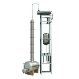
Alcohol Recovery Tower 1 Pieces / (Min. Order)
-
XH-112thicknessgauge 1 Pieces / (Min. Order)

-
JH Series Alcohol Recovery Tower 1 Pieces / (Min. Order)
-
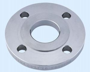
Astm 304 Slip On Flange 1 Pieces / (Min. Order)
-
Ricoh Aficio 1035/1045 1 Pieces / (Min. Order)

-
Ricoh Aficio MP2500/MP2500SP/MP2500SPF 1 Pieces / (Min. Order)

-
Ricoh Aficio 1015/1018/2015/2016/2018/2020 1 Pieces / (Min. Order)

-
Ricoh Aficio 1060/1075/2051/2060/2075 1 Pieces / (Min. Order)

-
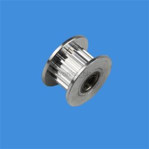
Alloy Timing Belt Pulley 1 Pieces / (Min. Order)
-
4ply Alcohol Sterile Non Woven Gauze Swabs 1 Pieces / (Min. Order)

-
A9 Processor 1 Pieces / (Min. Order)
-
Atmel Board 1 Pieces / (Min. Order)

-
Arm Development Board 1 Pieces / (Min. Order)
-
WM8962 Audio Module 1 Pieces / (Min. Order)
-
JH Series Alcohol Recovery Tower 1 Pieces / (Min. Order)
-
ABC-Acai Berry Slimming Capsule 1 Pieces / (Min. Order)

-
Bodyburn Catalyzer Slim Capsule 1 Pieces / (Min. Order)
-
Meizitang Strong Version Botanical Slimming Soft Gel 1 Pieces / (Min. Order)

-
MENOVA Qianweisu Herbs Capsule 1 Pieces / (Min. Order)

 Favorites
-
WM8962 Audio Module
1 Pieces / (Min. Order)
-
Arm Development Board
1 Pieces / (Min. Order)
-
Atmel Board
1 Pieces / (Min. Order)
-
A9 Processor
1 Pieces / (Min. Order)
 Frequent updates ensuring high quality data
 Over 5000 customers trust us to help grow their business!


 Menu
Menu