 Menu
Menu


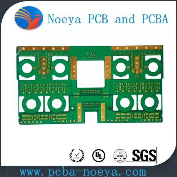


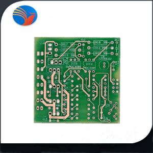
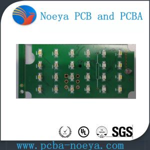
FR4 2 Layers Heavey Copper USB Bitcoin Miner
-
Min Order
1
-
Product Unit
Pieces
-
Origin
China Mainland
-
Payment


- Contact Now Start Order
- Favorites Share
- Description
Product Detail
FR4 2 Layers Heavey Copper USB Bitcoin Miner
Noeya is able to offer one-stop service 1-24 layer pcb and pcba, components sourcing, components assembly, function testing, reverse engineering and so on.
1. Description of the fr4 94v0 circuit board
Item: | fr4 94v0 circuit board |
Material: | FR-4 |
Board Thickness: | 1.6mm-5mm / Customized |
Copper Weight: | 6OZ |
Solder mask: | Green / Customized |
Silkscreen: | White / Customized |
Surface Finishing: | ENIG / OSP / HASL / Customized |
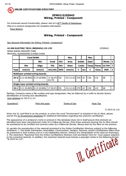
Certificate: | TS16949:2002, UL, ROHS, CE |
Flaming Rate: | 94v0 |
Quote requirements for pcb&pcb assembly:
For PCB:
---Gerber file, quantity and pcb specification
For PCBA:
---Gerber file, bomlist,
---quantity, testing method,
---Clear pictures of pcba or pcba sample
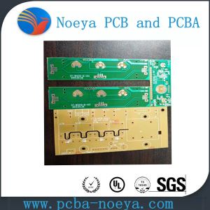
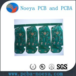
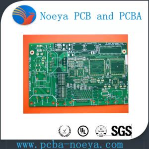
2. Noeya PCB Capability
Capability | Standard | Advanced |
FR4 / FR1 / CEM-3 / CEM-1 / Aluminum / Rigid-Flex PCB/ | ||
Laminate materials | Arlon / High-TG/ Rogers / Teflon / Taconic | |
HASL (vertical & Horizontal), Lead Free HASL, | ||
HASL+Gold Finger, | ||
OSP/Entek, | ||
Surface Finish | ENIG, ENEPIG, | |
Immersion Tin(ISn) ,Immersion Silver(IAg), | ||
Carbon Ink, | ||
Hard Gold(Flash Gold), Soft Gold | ||
Min. Thickness for inner layers | 0.020"-0.125" | 0.003”(0.07mm) |
Board layers | 1-24 Layers | 1-24 Layers |
Board Thickness | 0.1mm-3mm | 0.1mm-7mm |
Copper weight | 0.5 oz – 6 oz | 0.5 oz – 8 oz |
Minimum Trace Width / Spacing | 0.003"/0.003" | 0.003"/0.003" |
Solder Mask Color | Green,Blue,Black,Red,Yellow,White, and customized | |
Drill deviation | 0.004" | ±0.002” (0.05mm) |
PTH hole tolerance | 0.004" | ±0.002” (0.005mm) |
NPTH hole tolerance | 0.008" | ±0.002” (0.005mm) |
Min hole size | 0.004" | 0.008” (0.02mm) |
E-test | Flying Probe Tester/Test-Jig/X-ray/ICT/AOI/FCT | |
Controlled Tolerance | ±3% | ±3% |
Silkscreen Color | White, Black, Yellow, Green, Red, Blue and customized | |
Min solder mask clearance size | 0.008 | 0.003” (0.07mm) |
Min silkscreen clearance size | 0.010" | 0.006” (0.15mm) |
IPC Class | Class 2 | Class 3 |
Blind Vias | YES | YES |
Buried Vias | YES | YES |
Aspect Ratio | 8/1 | 15/1 |
Carbon Ink | YES | YES |
Peelable Mask | YES | YES |
Solder Sample | YES | YES |
First Article | YES | YES |
Certificate: | UL / SGS / ROH / ISO / TS16949 / ISO14001:2004 | |
Acceptable file format | GERBER file, PROTEL 99/PADS / POWER PCB / AutoCAD | |
/EAGLE | ||
3. Our Main Services
1). PCB (samples and mass products)
2). PCB Assembly
3).PCBA Copy & Reverse Engineering
4). Devices Sourcing
5). Function Test for PCB ASSEMBLY
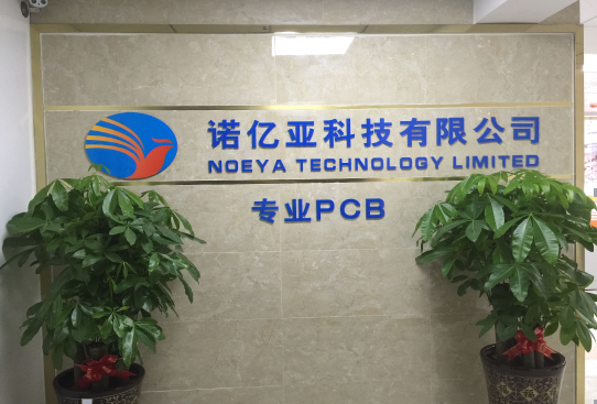
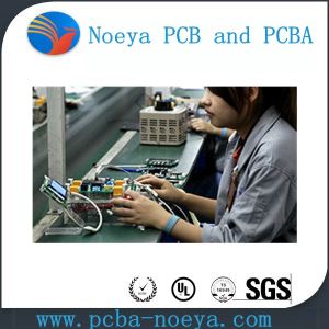
4. Our company
A Professional PCB & PCBA Manufacturer with 10 years’ experience
Our Factory
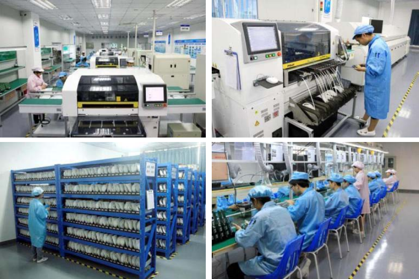
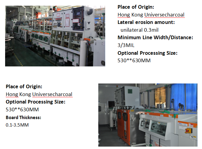
Our Products Equipment Introduction
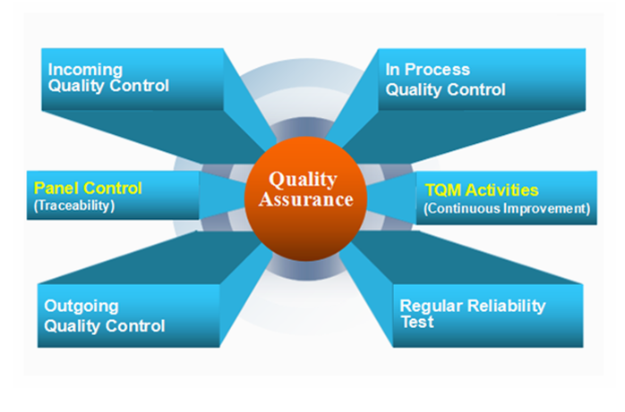
Our Quality Control System
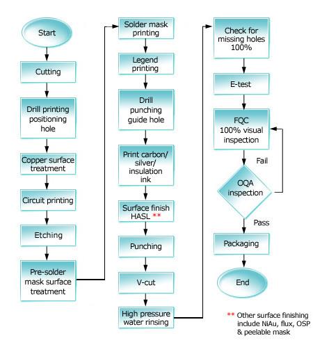
Our PCB & PCBA Manufacturing Flow Chart
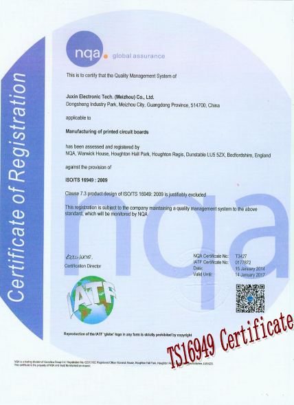
Our International Certificates
 |  |
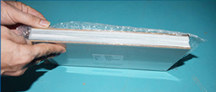
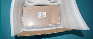
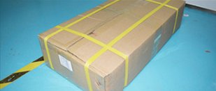
5. Packing
Vacuum packing for inner side:
 |  |
Carton packing for outer side:
 | 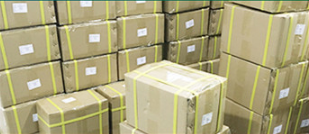 |
6. Shipping & Payment:Samples via DHL/UPS/FEDEX/TNT/EMS with short delivery time 2-4 working days.
Mass products via air/sea transportation at low shipping cost.

7. FAQ
Q: How can I get quotation in time?
A: Please send us the PCB File and Components list via mail or Online tool(Aliwangwang or Skype,WhatsApp)The file will be checked and the initial quotation will be offered withing 2 working days as usual(Gerber,Eagle,PCB,CAD file are acceptable).
Q: How to Place order ?
A:Step1: Send us the PO with request (Final project files confirmed) and we will confirm with PI.
Step2: The order will be entered into our order system in same day.
Step3: Deposit or full payment complete,then order confirmed by our financial department.
Step4: The order will be proceed accordingly by our purchasing system.
Step5: Sample or photos offered for approval.
Step6: Balance payment complete,shippment arranged and tracking will be offered via email.
Q: What's the normal sequency of order?
A:Step1:PCB board file with parts list details provided by customers.
Step2:PCB board file checked by PCB engineer.
Step3:PCB board components sourced by Zhengte Electronics.
Step4:Components checked by Zhengte Electronics warehouse stuffs.
Step4: PCB board with components assembled.
Step5: Electronic testing circuit board or PCBA.
Step6: Anti-static package,Fast delivery.
Q: How can make sure no mistake for mass production?
A: The production files will be checked by our engineering teams.Samples will be
offered for approval before mass production.
Q: What files in need for the PCB Assembly services?
A:Besides the PCB files and Components list,we also need PNP(Pick and Place)
and Components Position files for production.
Q: How can I track the shipment?
A:When order complete,an email will be sent out to confirm the value and shipment methods.
Then the shipment tracking number will be shared with email as always.
Q: How can I share the feedback?
A: Please send the comments with the order number within 30days to our feedback service department.Our service department will proceed in working days as usual.
8. Contact us
Shenzhen Noeya Technology Ltd.
| Salesman: Shirley Guo Email: sales06@noeya-pcb.com Skype: sales06_561 Tel: 0755-2955-3751/+8617673390006 Web:www.noeya-pcb.com
szczpcb.ec.alibaba.com |

-
Double-color Rotary Table Machines 1 Pieces / (Min. Order)
-
CA2000 Automatic Labeler Label Machine 1 Pieces / (Min. Order)
-
CB2000 Automatic Labeler Label Machine 1 Pieces / (Min. Order)
-
Unfolded Panel Material Butt Welder 1 Pieces / (Min. Order)
-
Roll On CNC Universal Machine 1 Pieces / (Min. Order)
-
Durable Flat Cable Reel With Factory Price 1 Pieces / (Min. Order)
-
Raw Material Mill 1 Pieces / (Min. Order)
-
Roll On CNC Universal Machine 1 Pieces / (Min. Order)
-
R-AP1188 Intercom Monitor Optical Transceiver 1 Pieces / (Min. Order)
-
HD-bag-type Dust Removal Machine 1 Pieces / (Min. Order)
-
Ribbon Da Maji (India-code) 1 Pieces / (Min. Order)
-
Double Tie Tie-ray Machine 1 Pieces / (Min. Order)
-
Raw Material Mill 1 Pieces / (Min. Order)
-
FR-60 Conveyor Belt Dust Removal Machine 1 Pieces / (Min. Order)
-
YLVC-2 Hay Cutter-type Sub-plate Machine Detail 1 Pieces / (Min. Order)
-
Weight TR2004 Multiplex Signal Transmitter 1 Pieces / (Min. Order)
-
YJ450HD rubber track pads-- CLIP ON RUBBER PAD 1 Pieces / (Min. Order)
-
YJ500K rubber track pads-- CHAIN ON RUBBER PAD 1 Pieces / (Min. Order)
-
YJ450B rubber track pads- BOLT ON RUBBER PAD 1 Pieces / (Min. Order)
-
Rugged Wall Phone for Kitchen JR202-FK 1 Pieces / (Min. Order)
 Favorites
-
 Tablet Circuit Board Pcb Supplier
1 Pieces / (Min. Order)
Tablet Circuit Board Pcb Supplier
1 Pieces / (Min. Order)
-
 Cem-1 94V0 Single Layer Sided PCB Circuit Board
1 Pieces / (Min. Order)
Cem-1 94V0 Single Layer Sided PCB Circuit Board
1 Pieces / (Min. Order)
-
 FR4 94V 0 1.6mm Carbon Ink Electronic1oz PCB
1 Pieces / (Min. Order)
FR4 94V 0 1.6mm Carbon Ink Electronic1oz PCB
1 Pieces / (Min. Order)
-
 HASL Lead Free Single Layer DIP LED Assembly PCB
1 Pieces / (Min. Order)
HASL Lead Free Single Layer DIP LED Assembly PCB
1 Pieces / (Min. Order)
-
 94V0 2 Layers Silver Smart Bare Ceramic PCB
1 Pieces / (Min. Order)
94V0 2 Layers Silver Smart Bare Ceramic PCB
1 Pieces / (Min. Order)
-
 Automation Air Conditioner Controller PCB
US $7.61-11.98 / Price
1 Pieces / (Min. Order)
 Frequent updates ensuring high quality data
 Over 5000 customers trust us to help grow their business!

 Menu
Menu