 Menu
Menu


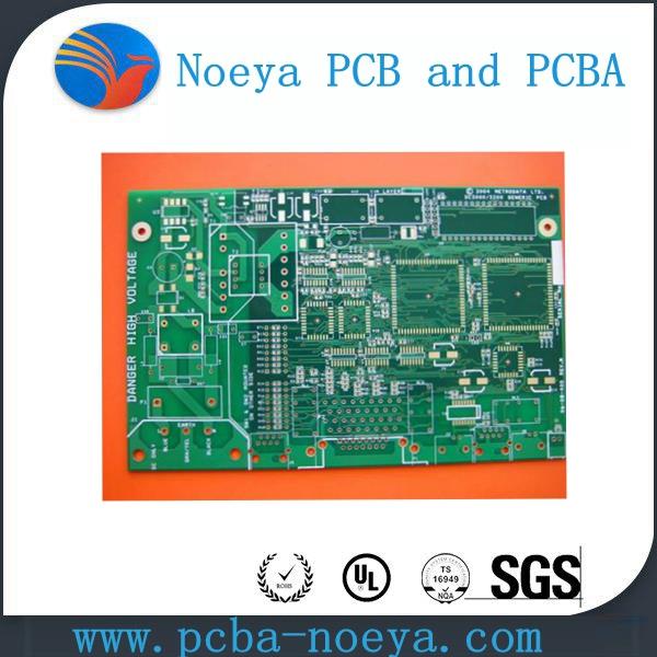


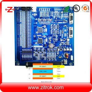
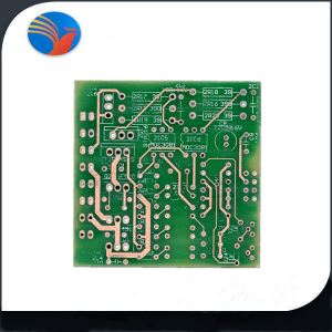
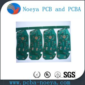
94V0 2 Layers Silver Smart Bare Ceramic PCB
-
Min Order
1
-
Product Unit
Pieces
-
Origin
China Mainland
-
Payment


- Contact Now Start Order
- Favorites Share
- Description
Product Detail
94V0 2 Layers Silver Smart Bare Ceramic PCB
Welcome to Shenzhen Noeya Technology Ltd.
We are professional manufacturer in Ru 94v0 double layers Immersion Silver Ceramic pcb boards with over 10 years’ experience. We prefer to supply our customers the best quality at the reasonable price.
1.Details of the Bare Ceramic pcb board
Item: | Bare Ceramic PCB board |
Material: | Ceramic |
Board Thickness: | 1.6mm / Customized |
Copper Weight: | 0.5OZ / Customized |
Solder mask: | Green / Blue / Customized |
Silkscreen: | White / Customized |
Surface Finishing: | Immersion Silver |
Min. Hole Size: | 0.2mm |
Min. Line Spacing: | 0.75mm |
Min. Trace Width: | 0.1mm |
Max. Aspect Ratio: | 8:1 |
Certificate: | TS16949:2002, UL, ROHS, CE |
Flaming Rate: | Ru 94v0 |
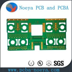
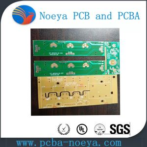
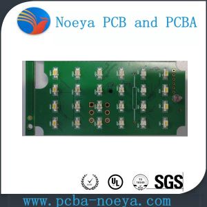
Details of PCB & PCBA
Technical requirement for pcb&pcb assembly:
---Professional Surface-mounting and Through-hole soldering Technology
---Various sizes like 1206,0805,0603 components SMT technology
---ICT(In Circuit Test),FCT(Functional Circuit Test) technology.
---PCB Assembly With UL,CE,FCC,Rohs Approval
---Nitrogen gas reflow soldering technology for SMT.
---High Standard SMT&Solder Assembly Line
---High density interconnected board placement technology capacity.
Quote requirement for pcb&pcb assembly:
---Gerber file and Bom list
---Clear pictures of pcba or pcba sample for us
---Test method for PCBA
2. Noeya Double layer PCB Capability
Capability | Standard | Advanced |
FR4 / FR1 / CEM-3 / CEM-1 / Aluminum / Rigid-Flex PCB/ | ||
Laminate materials | Arlon / High-TG/ Rogers / Teflon / Taconic | |
HASL (vertical & Horizontal), Lead Free HASL, | ||
HASL+Gold Finger, | ||
OSP/Entek, | ||
Surface Finish | ENIG, ENEPIG, | |
Immersion Tin(ISn) ,Immersion Silver(IAg), | ||
Carbon Ink, | ||
Hard Gold(Flash Gold), Soft Gold | ||
Min. Thickness for inner layers | 0.020"-0.125" | 0.003”(0.07mm) |
Board layers | 1-24 Layers | 1-24 Layers |
Board Thickness | 0.1mm-3mm | 0.1mm-7mm |
Copper weight | 0.5 oz – 6 oz | 0.5 oz – 8 oz |
Minimum Trace Width / Spacing | 0.003"/0.003" | 0.003"/0.003" |
Solder Mask Color | Green,Blue,Black,Red,Yellow,White, and customized | |
Drill deviation | 0.004" | ±0.002” (0.05mm) |
PTH hole tolerance | 0.004" | ±0.002” (0.005mm) |
NPTH hole tolerance | 0.008" | ±0.002” (0.005mm) |
Min hole size | 0.004" | 0.008” (0.02mm) |
E-test | Flying Probe Tester/Test-Jig/X-ray/ICT/AOI/FCT | |
Controlled Tolerance | ±3% | ±3% |
Silkscreen Color | White, Black, Yellow, Green, Red, Blue and customized | |
Min solder mask clearance size | 0.008 | 0.003” (0.07mm) |
Min silkscreen clearance size | 0.010" | 0.006” (0.15mm) |
IPC Class | Class 2 | Class 3 |
Blind Vias | YES | YES |
Buried Vias | YES | YES |
Aspect Ratio | 8/1 | 15/1 |
Carbon Ink | YES | YES |
Peelable Mask | YES | YES |
Solder Sample | YES | YES |
First Article | YES | YES |
Certificate: | UL / SGS / ROH / ISO / TS16949 / ISO14001:2004 | |
Acceptable file format | GERBER file, PROTEL 99/PADS / POWER PCB / AutoCAD | |
/EAGLE | ||
3. Our Advantages
1). PCB & PCBA ONE-STOP Services
2). Make high frequency and precision PCB (1-24 Layers)
3). Purchasing all components
4). Function e-testing
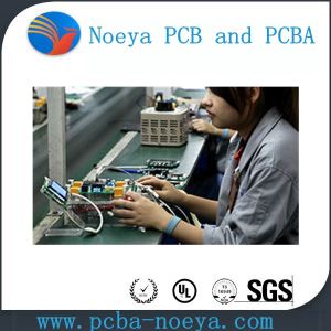
4. Our Factory and Machines Overview
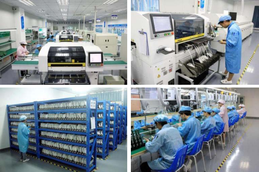
Our employees are all very professional in making pcb and pcba products. And there’s also complete quality control system in our company and factory. Meanwhile, our company are always practicing the environmental protection concept, our main raw materials are mainly from the world well-know environmental suppliers.
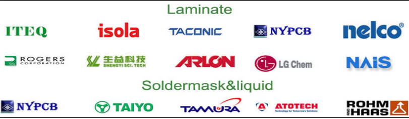
1). Our main raw material suppliers:
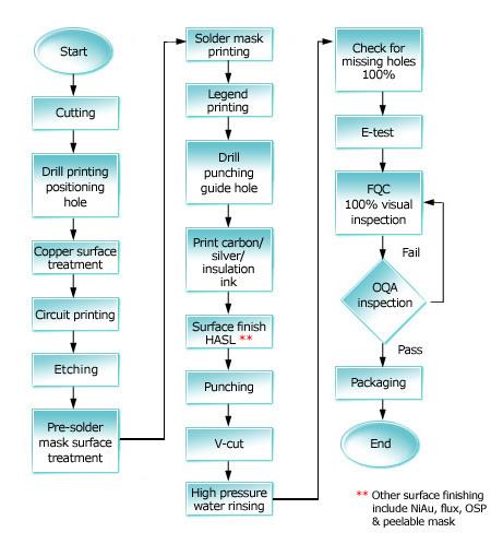
2). Our pcb and pcba manufacturing flow chart
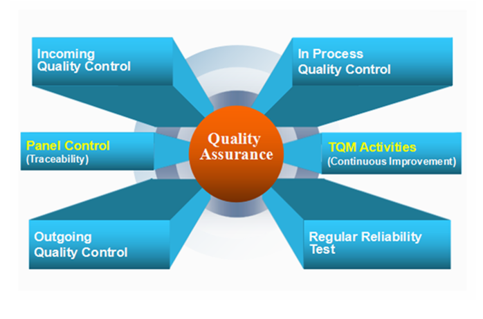
3). Our High precision quality control system
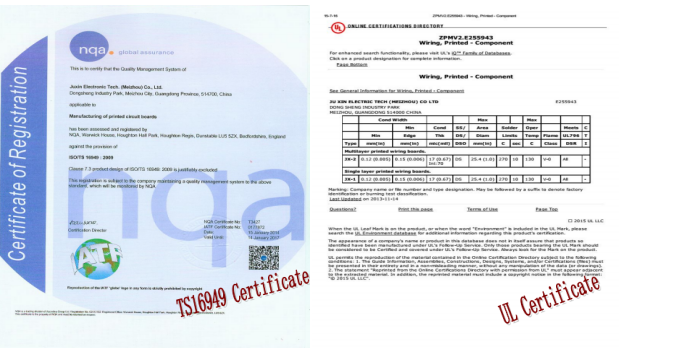
4). Our International Certificates
5. Packing & Shipping & Payment
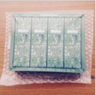
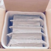
Inner side:Bulb vacuum package
 |  |
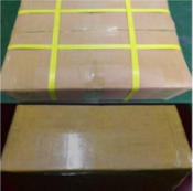
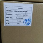
Outer side: Carton Package
 |  |
We cooperate with several famous express company, such as TNT, FEDEX, UPS, DHL, EMS and so on. Our customers can choose the way as you like.

6. FAQ
Q1: How do you make sure the quality of the PCBs?
A1: Our PCBs are all 100% test including Flying Probe Test, E-test or AOI.
Q2:What is your certificate?
A2: ISO/TS16949: 2000, ISO14001: 2004, UL, SGS, RoHS report. We can provide the report of raw material based on customer’s requirement.
Q3: What is the lead time?
A3: Sample needs 2-4 working days, mass production needs 7-10 working days. It depends on the files and quantity.
Q4: Do you keep our information and files secret?
A4: Keeping secret for customers is the basic principle of our factory. We can sign with the NDA with you.
Q5: What files should we offer?
A5: If only need PCBs, the Gerber files are needed; If need PCBA, both Gerber files and BOM are needed.
Q6: Can we visit your company?
A6: No problem. You are welcome to visit us in Shenzhen. And the other factory is in Meizhou City in Guangdong Province.
Q7: Can I get a sample?
A7: Yes, It's reasonable to get a sample to test our quality at first. But you have pay for the samples, and we will return half of the cost when the order is more than 20 sqm.
7. Contact us
Shenzhen Noeya Technology Ltd.
| Salesman: Shirley Guo Email: sales06@noeya-pcb.com Skype: sales06_561 Tel: 0755-2955-3751/+8617673390006 Web:www.noeya-pcb.com
szczpcb.ec.alibaba.com |

-
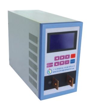
High Frequency Inverter Welding Power Source 1 Pieces / (Min. Order)
-
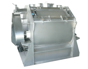
Zero-gravity Mixer RHL-0.15 Series 1 Pieces / (Min. Order)
-
EK Emirates Airline economy airline service 1 Pieces / (Min. Order)

-
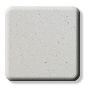
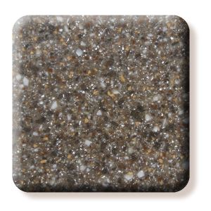
18mm Marble Patterned Solid Surface Acrylic Sheet 1 Pieces / (Min. Order)
-
Blue Solder Mask 52um Copper 4Layer Board With Assembly Service 1 Pieces / (Min. Order)
-
CE Approved Glacier White Acrylic Marble Stone Solid Surface 1 Pieces / (Min. Order)
-
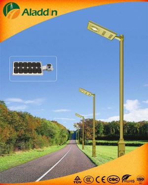
High-efficiency Integrated Solar Street Light 1 Pieces / (Min. Order)
-
Bathroom Shower Wall Panel , Texture Acrylic Solid Surface 1 Pieces / (Min. Order)
-
Brass Forged Integrated With Double Ball Valves 1 Pieces / (Min. Order)

-
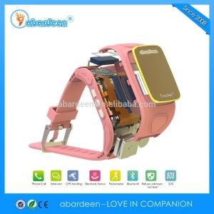
Voice Messages Intercom Kid GPS Tracker 1 Pieces / (Min. Order)
-
Carbon Bake Furnace In The Aluminum Industry Fire Brick 1 Pieces / (Min. Order)
-
12V 2500mA Power Adapter With Ul CE SAA BS Certificate 1 Pieces / (Min. Order)
-
Zirconium Tube/seamless Zr702 pipe/Welded Zr702 pipe/Zirconium pipe 1 Pieces / (Min. Order)
-
Hot Sale Factory Printed Tempered Glass Shower Screen 1 Pieces / (Min. Order)
-
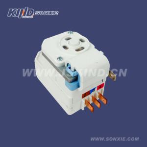
DBZ Defrost Timer Relay for Intelligent/Frost-free Refrigerator 1 Pieces / (Min. Order)
-
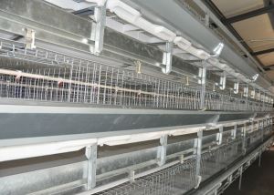
H Frame Broiler Battery Cage In Poultry Farm for Chicken 1 Pieces / (Min. Order)
-
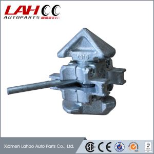
Container Intermediate Twist Lock (Left) 1 Pieces / (Min. Order)
-
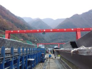
5 Ton 10 Ton Single Girder Gantry Crane Price 1 Pieces / (Min. Order)
-
Air-cooler Large Flat Tube Spray Aluminum 1 Pieces / (Min. Order)
 Favorites
-
 Tablet Circuit Board Pcb Supplier
1 Pieces / (Min. Order)
Tablet Circuit Board Pcb Supplier
1 Pieces / (Min. Order)
-
 FR4 2 Layers Heavey Copper USB Bitcoin Miner
1 Pieces / (Min. Order)
FR4 2 Layers Heavey Copper USB Bitcoin Miner
1 Pieces / (Min. Order)
-
 Cem-1 94V0 Single Layer Sided PCB Circuit Board
1 Pieces / (Min. Order)
Cem-1 94V0 Single Layer Sided PCB Circuit Board
1 Pieces / (Min. Order)
-
 FR4 94V 0 1.6mm Carbon Ink Electronic1oz PCB
1 Pieces / (Min. Order)
FR4 94V 0 1.6mm Carbon Ink Electronic1oz PCB
1 Pieces / (Min. Order)
-
 HASL Lead Free Single Layer DIP LED Assembly PCB
1 Pieces / (Min. Order)
HASL Lead Free Single Layer DIP LED Assembly PCB
1 Pieces / (Min. Order)
-
 Automation Air Conditioner Controller PCB
US $7.61-11.98 / Price
1 Pieces / (Min. Order)
 Frequent updates ensuring high quality data
 Over 5000 customers trust us to help grow their business!

 Menu
Menu